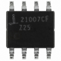
ISL21007CFB825Z-TK Intersil, ISL21007CFB825Z-TK Datasheet - Page 15

ISL21007CFB825Z-TK
Manufacturer Part Number
ISL21007CFB825Z-TK
Description
IC VOLT REF FGA LV 2.5V 8-SOIC
Manufacturer
Intersil
Series
FGA™r
Datasheet
1.ISL21007DFB812Z-TK.pdf
(18 pages)
Specifications of ISL21007CFB825Z-TK
Reference Type
Series
Voltage - Output
2.5V
Tolerance
±1mV
Temperature Coefficient
5ppm/°C
Voltage - Input
2.7 ~ 5.5 V
Number Of Channels
1
Current - Quiescent
150µA
Operating Temperature
-40°C ~ 125°C
Mounting Type
Surface Mount
Package / Case
8-SOIC (3.9mm Width)
Rohs Compliant
YES
Lead Free Status / RoHS Status
Lead free / RoHS Compliant
Current - Output
-
Current - Cathode
-
Other names
ISL21007CFB825Z-TKTR
Available stocks
Company
Part Number
Manufacturer
Quantity
Price
Company:
Part Number:
ISL21007CFB825Z-TK
Manufacturer:
Intersil
Quantity:
1 000
Typical Performance Curves (ISL21007-30)
Applications Information
FGA Technology
The ISL21007 voltage reference uses floating gate
technology to create references with very low drift and
supply current. Essentially, the charge stored on a floating
gate cell is set precisely in manufacturing. The reference
voltage output itself is a buffered version of the floating gate
voltage. The resulting reference device has excellent
characteristics which are unique in the industry: very low
temperature drift, high initial accuracy, and almost zero
supply current. Also, the reference voltage itself is not limited
by voltage bandgaps or zener settings, so a wide range of
reference voltages can be programmed (standard voltage
settings are provided, but customer-specific voltages are
available).
The process used for these reference devices is a floating
gate CMOS process, and the amplifier circuitry uses CMOS
transistors for amplifier and output transistor circuitry. While
providing excellent accuracy, there are limitations in output
noise level and load regulation due to the MOS device
characteristics. These limitations are addressed with circuit
techniques discussed in other sections.
Micropower Operation
The ISL21007 consumes extremely low supply current due
to the proprietary FGA technology. Low noise performance is
achieved using optimized biasing techniques. Supply current
is typically 75µA and noise is 4.5µV
low noise portable applications such as handheld meters
and instruments.
Data Converters in particular can utilize the ISL21007 as an
external voltage reference. Low power DAC and ADC
circuits will realize maximum resolution with lowest noise.
15
P-P
benefitting precision,
FIGURE 54. LOAD TRANSIENT RESPONSE
-7mA
ISL21007
(R
100µs/DIV
EXT
= 100kΩ) (Continued)
Board Mounting Considerations
For applications requiring the highest accuracy, board
mounting location should be reviewed. The device uses a
plastic SOIC package, which will subject the die to mild
stresses when the PC board is heated and cooled and
slightly change its shape. Placing the device in areas subject
to slight twisting can cause degradation of the accuracy of
the reference voltage due to these die stresses. It is normally
best to place the device near the edge of a board, or the
shortest side, as the axis of bending is most limited at that
location. Mounting the device in a cutout also minimizes flex.
Obviously, mounting the device on flexprint or extremely thin
PC material will likewise cause loss of reference accuracy.
Noise Performance and Reduction
The output noise voltage in a 0.1Hz to 10Hz bandwidth is
typically 4.5µV
bandpass filter made of a 1 pole high-pass filter with a corner
frequency at 0.1Hz and a 2-pole low-pass filter with a corner
frequency at 12.6Hz to create a filter with a 9.9Hz bandwidth.
Noise in the 10kHz to 1MHz bandwidth is approximately
40µV
measurement is made with a 2 decade bandpass filter made
of a 1 pole high-pass filter with a corner frequency at 1/10 of
the center frequency and 1-pole low-pass filter with a corner
frequency at 10 times the center frequency. Load capacitance
up to 1000pF can be added but will result in only marginal
improvements in output noise and transient response. The
output stage of the ISL21007 is not designed to drive heavily
capacitive loads, so for load capacitances above 0.001µF, the
noise reduction network shown in Figure 55 is recommended.
This network reduces noise significantly over the full
bandwidth. Noise is reduced to less than 20µV
1MHz using this network with a 0.01µF capacitor and a 2kΩ
resistor in series with a 10µF capacitor. Also, transient
response is improved with higher value output capacitor. The
0.01µF value can be increased for better load transient
response with little sacrifice in output stability.
P-P
+7mA
with no capacitance on the output. This noise
P-P
. The noise measurement is made with a
P-P
December 13, 2007
from 1Hz to
FN6326.7


