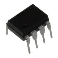
NJM4151D NJR, NJM4151D Datasheet - Page 4

NJM4151D
Manufacturer Part Number
NJM4151D
Description
IC V-F/F-V CONVERTER 8DIP
Manufacturer
NJR
Type
Volt to Freq & Freq to Voltr
Datasheet
1.NJM4151D.pdf
(10 pages)
Specifications of NJM4151D
Frequency - Max
100kHz
Full Scale
±100ppm/°C
Linearity
±1%
Mounting Type
Through Hole
Package / Case
8-DIP
Supply Voltage (max)
22 V
Supply Voltage (min)
8 V
Maximum Operating Temperature
+ 85 C
Minimum Operating Temperature
- 40 C
Full Scale Frequency
100 KHz
Mounting Style
Through Hole
Operating Supply Voltage
9 V, 12 V, 15 V, 18 V
Lead Free Status / RoHS Status
Contains lead / RoHS non-compliant
Available stocks
Company
Part Number
Manufacturer
Quantity
Price
Company:
Part Number:
NJM4151D
Manufacturer:
JRC
Quantity:
5 510
Company:
Part Number:
NJM4151D
Manufacturer:
MOT
Quantity:
5 510
Part Number:
NJM4151D
Manufacturer:
JRC
Quantity:
20 000
comparator, while Q8-Q11 and Q16-Q17 make up the R-S latch. One latch output, open-collector reset transistor Q16, is
connected to a comparator input and to the terminal, pin 5. Timing resistor R
capacitor C
comparator threshold voltage at 0.667V
latch. This causes Q16 to turn off, releasing the voltage at pin 5 to charge exponentially towards V
as this voltage reaches 0.667 V
reset, Q16 will discharge C
R
During the one-shot period the logic output will be in the low state. The one-shot output is also used to switch the
reference voltage by Q22 and Q24. The low T. C. reference voltage is derived from the combination of a 5.5V zener
diode with resistor and diode level shift networks. A stable 1.89 volts is developed at pin 2, the emitter of Q33.
and Q34. This current is reflected in the precision current mirror Q35-Q37 and produces the output current I
When the R-S latch is reset, Q22 and Q24 will hold the reference voltage off, pin 2 will be at 0V, and the current will be off.
During the one-shot period T, the latch will be set, the voltage of pin 2 will go to 1.89V, and the output current will be
switched on.
■ TYPICAL APPLICATION
1. Single supply Voltage-to-Frequency Converter
and output frequency is from 0 to 10kHz. Full scale frequency can be tuned by adjusting R
This circuit has the advantage of being simple and low in cost, but it suffers from inaccuracy due to a number of error
sources. Linearity error is typically 1%. A frequency offset will also be introduced by the input comparator offset voltage.
Also, response time for this circuit is limited by the passive integration network R
Figure 2, response time for a step change input from 0 to +10V will be 135msec. For applications which require fast
response time and high accuracy, use the circuits of Figure 3 and 4.
2. Precision VFC with Single Supply Voltage
circuit of Figure 3 will give greatly improved linearity, frequency offset, and response time. Here, an active integrator using
one section of the NJM3403A quad ground-sensing op-amp has replaced the R
for this circuit is due only to the NJM4151 current source output conductance. Frequency offset is due only to the op-amp
input offset and can be nulled to zero by adjusting R
voltage, so an op-amp with stable bias current, like the NJM3403A, is required.
Connecting the external current-setting resistor R
Figure 2 shows the simplest type of VFC that can be made with the NJM4151. Input voltage range is from 0 to +10V,
O
- 4 -
C
The one-shot is made from a voltage comparator and an R-S latch, Transistors Q12-Q15 and Q18-Q20 form the
For applications which require a VFC which will operate from a single positive supply with positive input voltage, the
O
at the latch output, Q21. This pulse is buffered through Q23 to drive the open-collector logic circuit transistor Q32.
O
is tied from pin 5 to ground. The other comparator input is tied to a voltage divider R
O
to ground. The one-shot has now completed its function of creating a pulse of period T=1.1
+
Figure 2. Single Supply Voltage-to-Frequency Converter
, comparator output Q20 will go high causing Q10 to reset the latch. When the latch is
+
. One-shot operation is initiated when the collector of Q7 goes low and sets the
S
= 14.0Ω from pin 2 to ground gives 135µA from the collectors of Q33
B
. This technique uses the op-amp bias current to develop the null
O
is tied externally from pin 5 to V
B
C
B
-C
B
. For the component values shown in
B
network in Figure 2. Linearity error
s
, the output current set resistor.
+
through R
3
-R
5
which sets the
Ver.2004-10-25
+
O
and timing
O
. As soon
at pin 1.


