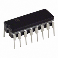
AD652AQ Analog Devices Inc, AD652AQ Datasheet - Page 7

AD652AQ
Manufacturer Part Number
AD652AQ
Description
IV V-F CONVERTER SYNC 16-CDIP
Manufacturer
Analog Devices Inc
Type
Voltage to Frequencyr
Specifications of AD652AQ
Rohs Status
RoHS non-compliant
Frequency - Max
2MHz
Full Scale
±50ppm/°C
Linearity
±0.02%
Mounting Type
Through Hole
Package / Case
16-CDIP (0.300", 7.62mm)
Full Scale Range
1MHz To 2MHz
Linearity %
0.02%
Supply Voltage Range
± 6V To ± 18V
Digital Ic Case Style
DIP
No. Of Pins
16
Frequency Max
2MHz
Termination Type
Through Hole
Converter Function
VFC
Full Scale Frequency
2000
Power Supply Requirement
Single/Dual
Single Supply Voltage (max)
36V
Single Supply Voltage (min)
12V
Dual Supply Voltage (typ)
±15V
Dual Supply Voltage (min)
±6V
Dual Supply Voltage (max)
±18V
Operating Temperature (min)
-40C
Operating Temperature (max)
85C
Operating Temperature Classification
Industrial
Package Type
CDIP
Converter Type
Voltage to Frequency
Current, Quiescent Supply
±11 mA (Typ.)
Frequency Range
5 MHz (Typ.)
Input Impedance
20 Kiloohms
Number Of Pins
20
Temperature, Operating, Maximum
85 °C
Temperature, Operating, Minimum
-40 °C
Voltage, Range
±6 to ±18 V
Voltage, Supply
36 V
Filter Terminals
Through Hole
Rohs Compliant
No
Calibration Error Fs Typ
5%
Lead Free Status / Rohs Status
Not Compliant
Available stocks
Company
Part Number
Manufacturer
Quantity
Price
Company:
Part Number:
AD652AQ
Manufacturer:
TOSHIBA
Quantity:
670
Figure 4 shows that the period between output pulses is
constrained to be an exact multiple of the clock period.
Consider an input current of exactly one quarter the value of
the reference current. In order to achieve a charge balance, the
output frequency equals the clock frequency divided by four:
one clock period for reset and three clock periods of integrate.
This is shown in Figure 5. If the input current is increased by a
very small amount, the output frequency should also increase
by a very small amount. Initially, however, no output change is
observed for a very small increase in the input current. The
output frequency continues to run at one quarter of the clock,
delivering an average of 250 µA to the summing junction. Since
the input current is slightly larger than this, charge accumulates
in the integrator and the sawtooth signal starts to drift down-
ward. As the integrator sawtooth drifts down, the comparator
threshold is crossed earlier and earlier in each successive cycle,
until finally, a whole cycle is lost. When the cycle is lost, the
integrate phase lasts for two periods of the clock instead of the
usual three periods. Thus, among a long string of divide-by-
fours, an occasional divide-by-three occurs; the average of the
output frequency is very close to one quarter of the clock, but
the instantaneous frequency can be very different.
V
IN
R
IN
COMPARATOR
INTEGRATOR
1mA
INTEGRATOR
OUTPUT
D FLOP
CLOCK
H
LATCH
–V
FREQ
AND
OUT
OUT
OUT
OUT
OUT
Figure 4. Block Diagram and System Waveforms
S
L
C
INT
COMPARATOR
5V
Rev. C | Page 7 of 28
t
OS
THRESHOLD
AND
D FLOP
INTEGRATOR
Because of this, it is very difficult to observe the waveform on
an oscilloscope. During all of this time, the signal at the output
of the integrator is a sawtooth wave with an envelope that is also
a sawtooth. See Figure 6.
D
CLOCK IN
CK
CLOCK
Q
OUT
Figure 6. Integrator Output for I
D
G Q
LATCH
Q
t
Figure 5. Integrator Output for I
OS
THRESHOLD
SHOT
ONE
C
OS
IN
Slightly Greater than 250 µs
IN
= 250 µA
200µs/BOX
100µs/BOX
FREQ OUT
10µs/BOX
CLOCK IN
10µs/BOX
AD652
C
INT


