ADVFC32BH Analog Devices Inc, ADVFC32BH Datasheet - Page 3
ADVFC32BH
Manufacturer Part Number
ADVFC32BH
Description
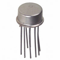
IC CONV V/F F/V MONO TO100-10
Manufacturer
Analog Devices Inc
Type
Volt to Freq & Freq to Voltr
Datasheet
1.ADVFC32KNZ.pdf
(6 pages)
Specifications of ADVFC32BH
Rohs Status
RoHS non-compliant
Frequency - Max
500kHz
Full Scale
±100ppm/°C
Linearity
±0.05%
Mounting Type
Through Hole
Package / Case
TO-100-10 Metal Can
Frequency
500kHz
Full Scale Range
0kHz To 500kHz
Linearity %
0.005%
Supply Voltage Range
± 9V To ± 18V
Digital Ic Case Style
TO-100
No. Of Pins
10
Msl
MSL 1 - Unlimited
Converter Function
VFC/FVC
Full Scale Frequency
500
Power Supply Requirement
Dual
Single Supply Voltage (typ)
Not RequiredV
Single Supply Voltage (max)
Not RequiredV
Single Supply Voltage (min)
Not RequiredV
Dual Supply Voltage (typ)
±15V
Dual Supply Voltage (min)
±9V
Dual Supply Voltage (max)
±18V
Operating Temperature (min)
-25C
Operating Temperature (max)
85C
Operating Temperature Classification
Commercial
Package Type
TO-100
Lead Free Status / Rohs Status
Not Compliant
Available stocks
Company
Part Number
Manufacturer
Quantity
Price


CAUTION
ESD (electrostatic discharge) sensitive device. Electrostatic charges as high as 4000 V readily
accumulate on the human body and test equipment and can discharge without detection. Although
the ADVFC32 features proprietary ESD protection circuitry, permanent damage may occur on
devices subjected to high-energy electrostatic discharges. Therefore, proper ESD precautions are
recommended to avoid performance degradation or loss of functionality.
UNIPOLAR V/F, POSITIVE INPUT VOLTAGE
When operated as a V/F converter, the transformation from
voltage to frequency is based on a comparison of input signal
magnitude to the 1 mA internal current source.
A more complete understanding of the ADVFC32 requires a
close examination of the internal circuitry of this part. Consider
the operation of the ADVFC32 when connected as shown in
Figure 1. At the start of a cycle, a current proportional to the
input voltage flows through R3 and R1 to charge integration
capacitor C2. As charge builds up on C2, the output voltage of
the input amplifier decreases. When the amplifier output volt-
age (Pin 13) crosses ground (see Figure 2 at time t
comparator triggers a one shot whose time period is determined
by capacitor C1. Specifically, the one shot time period (in nano-
seconds) is:
During this period, a current of (1 mA – I
integration capacitor. The total amount of charge depleted
during one cycle is, therefore (1 mA – I
t
OS
≅ (C
l
+ 44 pF) × 6.7 kΩ
IN
) × t
IN
) flows out of the
OS
. This charge is
1
), the
replaced during the remainder of the cycle to return the integra-
tor to its original voltage. Since the charge taken out of C2 is
equal to the charge that is put on C2 every cycle,
or, rearranging terms,
The complete transfer equation can now be derived by substi-
tuting I
final equation describing ADVFC32 operation is:
Components should be selected to optimize performance over
the desired input voltage and output frequency range using the
equations listed below:
Both R
as changes in their values will result in a proportionate change
in the V/F transfer function. Other component values and tem-
perature coefficients are not critical.
V
1 V
10 V
1 V
10 V
Part
Number
ADVFC32KN
ADVFC32BH
ADVFC32SH
NOTE
1
For details on grade and package offerings screened in accordance with MIL-STD-883,
refer to the Analog Devices Military Products Databook or current ADVFC32/883B
data sheet.
IN FS
(1 mA – I
F
C
R
R
1mA × C
3.7 ×10
OUT
IN
2
2
IN
IN
=
≥
=
1
F
Table I. Suggested Values for C
and C
= V
10
+V
=
F
10 kHz
10 kHz
100 kHz
100 kHz
OUT FS
0.25 mA
V
8 mA
OUT FS
(
7
–4
1 mA × t
LOGIC
IN
IN FS
IN
V
F
1
pF / sec
Farads / sec
/R
1
) × t
II N
OUT FS
+ 44 pF
I
should have very low temperature coefficients
IN
IN
Gain Tempco
ppm/ C
± 75 typ
± 100 max
± 150 max
/ R
OS
and the equation relating C1 and t
ORDERING GUIDE
OS
IN
– 44 pF
= I
)
× 6.7 kΩ
C
3650 pF
3650 pF
330 pF
330 pF
IN
1
(
1000 pF minimum
×
F
OUT
1
WARNING!
Temp Range
0 to 70
–25 to +85
–55 to +125
C
– t
R
4.0 kΩ
40 kΩ
4.0 kΩ
40 kΩ
IN
OS
1
, R
ESD SENSITIVE DEVICE
IN
)
and C
ADVFC32
C
0.01 µF
0.01 µF
1000 pF
1000 pF
2
Package
Option
14-Pin
Plastic DIP
TO-100
TO-100
2
OS
. The
Related parts for ADVFC32BH
Image
Part Number
Description
Manufacturer
Datasheet
Request
R

Part Number:
Description:
±1.7g Dual-Axis IMEMS Accelerometer Evaluation Board
Manufacturer:
Analog Devices Inc
Datasheet:

Part Number:
Description:
Inertial Sensor Evaluation System
Manufacturer:
Analog Devices Inc
Datasheet:
Part Number:
Description:
Manufacturer:
Analog Devices Inc
Datasheet:
Part Number:
Description:
Manufacturer:
Analog Devices Inc
Datasheet:
Part Number:
Description:
Manufacturer:
Analog Devices Inc
Datasheet:
Part Number:
Description:
Manufacturer:
Analog Devices Inc
Datasheet:
Part Number:
Description:
Manufacturer:
Analog Devices Inc
Datasheet:
Part Number:
Description:
Manufacturer:
Analog Devices Inc
Datasheet:
Part Number:
Description:
Manufacturer:
Analog Devices Inc
Datasheet:
Part Number:
Description:
Manufacturer:
Analog Devices Inc
Datasheet:
Part Number:
Description:
Manufacturer:
Analog Devices Inc
Datasheet:
Part Number:
Description:
Manufacturer:
Analog Devices Inc
Datasheet:
Part Number:
Description:
Manufacturer:
Analog Devices Inc
Datasheet: