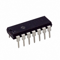
TC9402CPD Microchip Technology, TC9402CPD Datasheet - Page 7

TC9402CPD
Manufacturer Part Number
TC9402CPD
Description
IC V-FREQ/FREQ-V CONV 14DIP
Manufacturer
Microchip Technology
Type
Volt to Freq & Freq to Voltr
Specifications of TC9402CPD
Package / Case
14-DIP (0.300", 7.62mm)
Frequency - Max
100kHz
Full Scale
±100ppm/°C
Linearity
±0.25%
Mounting Type
Through Hole
Supply Voltage (max)
15 V
Supply Voltage (min)
8 V
Maximum Operating Temperature
70 C
Minimum Operating Temperature
0 C
Dual Supply Voltage
+/- 5 V
Full Scale Frequency
100 KHz
Linearity Error
+/- 0.5 % FSR
Maximum Dual Supply Voltage
+/- 7.5 V
Minimum Dual Supply Voltage
+/- 4 V
Mounting Style
Through Hole
Operating Supply Voltage
9 V or 12 V
Frequency
100kHz
Full Scale Range
1Hz To 100kHz
Linearity %
0.25%
Supply Voltage Range
± 4V To ± 7.5V
Digital Ic Case Style
DIP
No. Of Pins
14
Frequency Max
100kHz
Rohs Compliant
Yes
Lead Free Status / RoHS Status
Lead free / RoHS Compliant
Lead Free Status / RoHS Status
Lead free / RoHS Compliant, Lead free / RoHS Compliant
Other names
158-1142
158-1142
158-1142
2.6
This output is an open-drain N-channel FET, which
provides a pulse waveform whose frequency is propor-
tional to the input voltage. This output requires a pull-
up resistor and interfaces directly with MOS, CMOS,
and TTL logic (see
2.7
The sources of both the FREQ/2 OUT and the PULSE
FREQ OUT are connected to this pin. An output level
swing from the drain voltage to ground, or to the V
supply, may be obtained by connecting this pin to the
appropriate point.
2.8
This output is an open-drain N-channel FET, which
provides a square-wave one-half the frequency of the
pulse frequency output. The FREQ/2 OUT output will
change state on the rising edge of PULSE FREQ OUT.
This output requires a pull-up resistor and interfaces
directly with MOS, CMOS, and TTL logic.
FIGURE 2-1:
© 2007 Microchip Technology Inc.
F
Amp Out
OUT
F
Note 1: To adjust F
OUT
/2
Pulse Freq Out
Output Common
Freq/2 Out
2: To adjust F
3: To increase F
4: For high performance applications, use high stability components for R
resistors and glass capacitors). Also, separate output ground (Pin 9) from input ground (Pin 6).
Figure
Output Waveforms.
MIN
MAX
2-1).
1/f
OUTMAX
, set V
, set V
IN
3 ms
Typ.
IN
to 100 kHz, change C
= 10 mV and adjust the 50 kΩ offset for 10 Hz output.
= 10V and adjust R
SS
IN
REF
or V
to 2 pF and C
2.9
In the V/F mode, this input is connected to the AMPLI-
FIER OUT output (Pin 12) and triggers a 3 µs pulse
when the input voltage passes through its threshold. In
the F/V mode, the input frequency is applied to this
input.
The nominal threshold of the detector is half way
between the power supplies, or (V
mV. The TC9400’s charge balancing V/F technique is
not dependent on a precision comparator threshold,
because the threshold only sets the lower limit of the op
amp output. The op amp’s peak-to-peak output swing,
which determines the frequency, is only influenced by
external capacitors and by V
2.10
This pin is the output stage of the operational amplifier.
During V/F operation, a negative going ramp signal is
available at this pin. In the F/V mode, a voltage
proportional to the frequency input is generated.
REF
for 10 kHz output.
TC9400/9401/9402
Threshold Detector Input
Amplifier Out
INT
to 75 pF.
IN
, C
REF
REF
.
. V
DD
REF
DS21483D-page 7
V REF
0V
+ V
(metal film
SS
C REF
C INT
)/2 ±400


