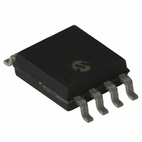
TCN75-5.0MOA713G Microchip Technology, TCN75-5.0MOA713G Datasheet - Page 3

TCN75-5.0MOA713G
Manufacturer Part Number
TCN75-5.0MOA713G
Description
IC TEMP SENSOR SRL 5.0V 8SOIC
Manufacturer
Microchip Technology
Specifications of TCN75-5.0MOA713G
Function
Temp Monitoring System (Sensor)
Topology
ADC (Sigma Delta), Register Bank
Sensor Type
Internal
Sensing Temperature
-55°C ~ 125°C
Output Type
2-Wire Serial
Output Alarm
Yes
Output Fan
No
Voltage - Supply
2.7 V ~ 5.5 V
Operating Temperature
-55°C ~ 125°C
Mounting Type
Surface Mount
Package / Case
8-SOIC (3.9mm Width)
Temperature Threshold
Programmable
Full Temp Accuracy
3 C
Digital Output - Bus Interface
2-Wire
Digital Output - Number Of Bits
9 bit
Supply Voltage (max)
5.5 V
Supply Voltage (min)
2.7 V
Description/function
2-Wire Serial Input/Output - Thermal Monitors
Maximum Operating Temperature
+ 125 C
Minimum Operating Temperature
- 55 C
Supply Current
1 mA
Lead Free Status / RoHS Status
Lead free / RoHS Compliant
1.0
Absolute Maximum Ratings*
Supply Voltage (V
ESD Susceptibility (Note 3) ............................... 1000V
Voltage on Pins:
Voltage on Pins:
Thermal Resistance (Junction to Ambient)
Operating Temperature Range (T
Storage Temperature Range (T
TCN75 ELECTRICAL SPECIFICATIONS
© 2006 Microchip Technology Inc.
Electrical Characteristics: V
Power Supply
INT/CMPTR Output
Temp-to-Bits Converter
t
T
T
2-Wire Serial Bus Interface
V
V
V
C
I
I
CONV
LEAK
OL(SDA)
Symbol
SET(PU)
HYST(PU)
IH
IL
OL
IN
t
I
V
V
I
TRIP
DD1
I
ΔT
DD
OL
DD
OL
A0, A1, A2 .......... (GND – 0.3V) to (V
SDA, SCL, INT/CMPTR .. (GND – 0.3V) to 5.5V
8-Pin SOIC.......................................... 170°C/W
8-Pin MSOP ....................................... 250°C//W
ELECTRICAL
CHARACTERISTICS
Power Supply Voltage
Operating Current
Standby Supply Current
Sink Current: INT/CMPTR,
SDA Outputs
INT/CMPTR Response Time
Output Low Voltage
Temperature Accuracy (Note 2)
Conversion Time
TEMP Default Value
T
Logic Input High
Logic Input Low
Logic Output Low
Input Capacitance SDA, SCL
I/O Leakage
SDA Output Low Current
HYST
DD
Default Value
) ............................................ 6.0V
Parameter
DD
= 2.7V – 5.5V, -55°C ≤ (T
STG
J
): -55°C to +125°C
): -65°C to +150°C
DD
V
+ 0.3V)
DD
Min
2.7
—
—
—
—
—
—
—
—
—
—
—
—
—
—
—
1
x 0.7
A
= T
J
0.250
) ≤ 125°C, unless otherwise noted.
±100
±0.5
Typ
±3
55
80
75
15
—
—
—
—
—
—
—
—
1
1
*Stresses
Maximum Ratings” may cause permanent damage to
the device. These are stress ratings only and functional
operation of the device at these or any other conditions
above those indicated in the operation sections of the
specifications is not implied. Exposure to Absolute
Maximum Rating conditions for extended periods may
affect device reliability.
V
DD
Max
5.5
1.0
0.8
0.4
—
—
—
±3
—
—
—
—
—
—
4
6
6
x 0.3
above
Units
t
msec
CONV
mA
mA
mA
μA
°C
°C
°C
°C
pF
pA
—
V
V
V
V
Serial Port Inactive (T
Serial Port Active
Shutdown Mode, Serial Port
Inactive (T
Note 1
User Programmable
I
-55°C ≤ T
V
TCN75-3.3 MUA
V
TCN75-5.0 MUA
25°C ≤ T
Power-up
Power-up
I
(T
OL
OL
those
DD
DD
A
= 4.0 mA
= 3 mA
= T
= 3.3V: TCN75-3.3 MOA,
= 5.0V: TCN75-5.0 MOA,
J
= 25°C)
A
A
listed
Test Conditions
A
≤ 100°C
≤ +125°C
= T
J
= 25°C)
under
TCN75
DS21490C-page 3
A
= T
J
“Absolute
= 25°C)


