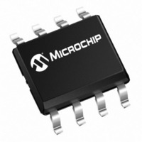
TCN75-3.3MUA Microchip Technology, TCN75-3.3MUA Datasheet - Page 7

TCN75-3.3MUA
Manufacturer Part Number
TCN75-3.3MUA
Description
IC TEMP SENSOR SRL 3.3V 8MSOP
Manufacturer
Microchip Technology
Datasheets
1.TCN75-5.0MUA.pdf
(20 pages)
2.TCN75-5.0MOA.pdf
(18 pages)
3.TCN75-5.0MUA.pdf
(30 pages)
4.TCN75AVOA.pdf
(30 pages)
Specifications of TCN75-3.3MUA
Package / Case
8-MSOP, Micro8™, 8-uMAX, 8-uSOP,
Output Type
2-Wire Serial
Function
Temp Monitoring System (Sensor)
Topology
ADC (Sigma Delta), Register Bank
Sensor Type
Internal
Sensing Temperature
-55°C ~ 125°C
Output Alarm
Yes
Output Fan
No
Voltage - Supply
2.7 V ~ 5.5 V
Operating Temperature
-55°C ~ 125°C
Mounting Type
Surface Mount
Temperature Threshold
Programmable
Full Temp Accuracy
3 C
Digital Output - Bus Interface
2-Wire
Digital Output - Number Of Bits
9 bit
Supply Voltage (max)
5.5 V
Supply Voltage (min)
2.7 V
Description/function
2-Wire Serial Input/Output - Thermal Monitors
Maximum Operating Temperature
+ 125 C
Minimum Operating Temperature
- 55 C
Supply Current
1 mA
Ic Output Type
Logic
Sensing Accuracy Range
± 0.5°C
Supply Voltage Range
2.7V To 5.5V
Sensor Case Style
MSOP
No. Of Pins
8
Filter Terminals
SMD
Rohs Compliant
Yes
Accuracy %
0.5°C
Lead Free Status / RoHS Status
Lead free / RoHS Compliant
Lead Free Status / RoHS Status
Lead free / RoHS Compliant, Lead free / RoHS Compliant
Other names
158-1003
158-1003
158-1003
Available stocks
Company
Part Number
Manufacturer
Quantity
Price
Part Number:
TCN75-3.3MUA
Manufacturer:
MICROCHIP/微芯
Quantity:
20 000
3.0
The descriptions of the pins are listed in Table 3-1.
TABLE 3-1:
3.1
SDA is a bidirectional input/output pin, used to serially
transmit data to and from the host controller. This pin
requires a pull-up resistor to output data.
3.2
SCLK is a clock input pin. All communication and timing
is relative to the signal on this pin. The clock is
generated by the host controller on the bus.
3.3
V
specified in the DC electrical specification table, is
applied on this pin.
3.4
GND is the system ground pin.
© 2005 Microchip Technology Inc.
DD
MSOP, SOIC
is the power pin. The operating voltage, as
PIN DESCRIPTION
Serial Data Pin (SDA)
Serial Clock Pin (SCLK)
Power Supply Input (V
Ground (GND)
1
2
3
4
5
6
7
8
PIN FUNCTION TABLE
Symbol
ALERT
SCLK
GND
SDA
V
A2
A1
A0
DD
DD
Bidirectional Serial Data
Serial Clock Input
Temperature Alert Output
Ground
Address Select Pin (bit 2)
Address Select Pin (bit 1)
Address Select Pin (bit 0)
Power Supply Input
)
3.5
The TCN75A’s ALERT pin is an open-drain output. The
device outputs an alert signal when the ambient
temperature goes beyond the user-programmed
temperature limit.
3.6
A2, A1 and A0 are device or slave address input pins.
The address pins are the Least Significant bits (LSb) of
the device address bits. The Most Significant bits
(MSb) (A6, A5, A4, A3) are factory-set to <1001>. This
is illustrated in Table 3-2.
TABLE 3-2:
TCN75A
Note:
Device
ALERT Output
Address Pins (A2, A1, A0)
Function
User-selectable address is shown by X.
SLAVE ADDRESS
A6
1
A5
0
A4
0
TCN75A
A3
1
DS21935A-page 7
A2
X
A1
X
A0
X


