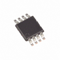
DS1825U+ Maxim Integrated Products, DS1825U+ Datasheet - Page 8

DS1825U+
Manufacturer Part Number
DS1825U+
Description
IC THERMOMETER DIGITAL 8-USOP
Manufacturer
Maxim Integrated Products
Datasheet
1.DS1825U.pdf
(21 pages)
Specifications of DS1825U+
Function
Thermometer, Thermostat
Topology
Register Bank, Scratchpad
Sensor Type
Internal
Sensing Temperature
-55°C ~ 125°C
Output Type
Digital
Output Alarm
Yes
Output Fan
No
Voltage - Supply
3 V ~ 3.7 V
Operating Temperature
-55°C ~ 125°C
Mounting Type
Surface Mount
Package / Case
8-MSOP, Micro8™, 8-uMAX, 8-uSOP,
Temperature Threshold
Programmable
Full Temp Accuracy
+/- 0.5 C
Digital Output - Bus Interface
1-Wire
Digital Output - Number Of Bits
9 bit to 12 bit
Supply Voltage (max)
3.7 V
Supply Voltage (min)
3 V
Maximum Operating Temperature
+ 125 C
Minimum Operating Temperature
- 55 C
Supply Current
1.5 mA
Ic Output Type
Digital
Sensing Accuracy Range
± 0.5°C
Supply Voltage Range
3V To 3.7V
Resolution (bits)
12bit
Sensor Case Style
µSOP
No. Of Pins
8
Accuracy %
0.5°C
Rohs Compliant
Yes
Lead Free Status / RoHS Status
Lead free / RoHS Compliant
Byte 8 of the scratchpad is read-only and contains the cyclic redundancy check (CRC) code for bytes 0 through 7
of the scratchpad. The DS1825 generates this CRC using the method described in the CRC GENERATION
section.
Data is written to bytes 2, 3, and 4 of the scratchpad using the Write Scratchpad [4Eh] command; the data must be
transmitted to the DS1825 starting with the least significant bit of byte 2. To verify data integrity, the scratchpad can
be read (using the Read Scratchpad [BEh] command) after the data is written. When reading the scratchpad, data
is transferred over the 1-Wire bus starting with the least significant bit of byte 0. To transfer the T
configuration data from the scratchpad to EEPROM, the master must issue the Copy Scratchpad [48h] command.
Data in the EEPROM registers is retained when the device is powered down; at power-up the EEPROM data
(including the hard-wired address inputs AD0-AD3)is reloaded into the corresponding scratchpad locations. Data
can also be reloaded from EEPROM to the scratchpad at any time using the Recall E
can issue read time slots following the Recall E
transmitting 0 while the recall is in progress and 1 when the recall is done.
Figure 7. DS1825 MEMORY MAP
CONFIGURATION REGISTER
Byte 4 of the scratchpad memory is the configuration register, as shown in Figure 8. The configuration register
allows the user to set the conversion resolution using the R0 and R1 bits and read the programmed value of the
address pins. The conversion resolution power-up default is R0 = 1 and R1 = 1 (12-bit resolution). Table 4 shows
the resolution configuration settings and maximum conversion time. Note that there is a direct tradeoff between
resolution and conversion time. AD0-AD3 bits report the pin programmed location information and are sampled at
power-up. In Parasite Power mode, the address pins must be connected to DQ or GND and in V
the address pins must be connected to V
to GND are reported as a logical 0. Pins connected to DQ/ V
logical 0s if the resistor is less than 10k. Floating or high impedance (>10kW) connections are indeterminate. Bit 7
and Bit 4 of the configuration register are reserved for internal use and cannot be overwritten.
Figure 8. CONFIGURATION REGISTER FORMAT
Note: Bit 0 through Bit 3 are programmed through the four Location Programming Address pins AD0-AD3.
Reading the configuration register provides location information on up to 16 individual DS1825s.
byte 0
byte 1
byte 2
byte 3
byte 4
byte 5
byte 6
byte 7
byte 8
* Lower four bits of Configuration Register
Temperature LSB (50h)
Temperature MSB (05h)
T
T
Configuration Register*
Reserved
Reserved
Reserved
CRC
H
L
Register or User Byte 2
Register or User Byte 1
SCRATCHPAD (Power-up State)
are hardwired through AD0-AD3
bit 7
0
bit 6
R1
DD
bit 5
R0
or GND. Pins tied to DQ/V
2
command and the DS1825 will indicate the status of the recall by
bit 4
(85°C)
1
8 of 21
bit 3
AD3
DD
or GND through a resistor are valid logical 1s or
AD2
bit 2
DD
are reported with a logical 1 and pins tied
bit 1
AD1
T
T
H
L
Configuration Register*
Register or User Byte 2
Register or User Byte 1
2
[B8h] command. The master
AD0
bit 0
EEPROM
DD
powered mode,
H
, T
L
, and


