AD637JQ Analog Devices Inc, AD637JQ Datasheet - Page 10
AD637JQ
Manufacturer Part Number
AD637JQ
Description
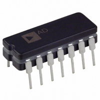
IC RMS/DC CONV PRECISION 14-CDIP
Manufacturer
Analog Devices Inc
Specifications of AD637JQ
Rohs Status
RoHS non-compliant
Current - Supply
2.2mA
Voltage - Supply
±3.0V ~ 18V
Mounting Type
Through Hole
Package / Case
14-CDIP (0.300", 7.62mm)
Accuracy %
0.25%
Bandwidth
200kHz
Supply Current
2.2mA
Power Dissipation Pd
108mW
Supply Voltage Range
± 3V To ± 18V
Digital Ic Case Style
DIP
No. Of Pins
14
Input Type
RMS
Module Type
Converter
Output Type
DC
Voltage, Supply
± 18 VDC
For Use With
AD637-EVALZ - BOARD EVALUATION FOR AD637
Lead Free Status / RoHS Status
Contains lead / RoHS non-compliant
Available stocks
Company
Part Number
Manufacturer
Quantity
Price

Part Number:
AD637JQ
Manufacturer:
ADI/亚德诺
Quantity:
20 000
Company:
Part Number:
AD637JQZ
Manufacturer:
NS
Quantity:
6 221


Figure 17 is a curve of additional reading error for the AD637
for a 1 V rms input signal with crest factors from 1 to 11. A
rectangular pulse train (pulse width 100 µs) was used for this
test because it is the worst-case waveform for rms measurement
(all the energy is contained in the peaks). The duty cycle and
peak amplitude were varied to produce crest factors from l to 10
while maintaining a constant 1 V rms input amplitude.
0.01
–0.5
–1.0
–1.5
0.1
1.5
1.0
0.5
10
1
0
0
1
1
Vp
Figure 16. AD637 Error vs. Pulse Width Rectangular Pulse
100
POSITIVE INPUT PULSE
µ
2
F
T
Figure 17. Additional Error vs. Crest Factor
C
AV
3
e
0
= 22 µ F
4
10
PULSE WIDTH ( µ s)
CREST FACTOR
e
5
η
CF = 1/
IN
= DUTY CYCLE =
(RMS) = 1 V RMS
6
η
7
100
100
T
8
µ
C
s
AV
CF = 10
9
= 22 µ F
CF = 3
10
1000
1
1
Rev. G | Page 13 of 20
CONNECTION FOR DB OUTPUT
Another feature of the AD637 is the logarithmic, or decibel,
output. The internal circuit that computes dB works well over a
60 dB range. Figure 19 shows the dB measurement connection.
The user selects the 0 dB level by setting R1 for the proper 0 dB
reference current, which is set to exactly cancel the log output
current from the squarer/divider circuit at the desired 0 dB
point. The external op amp is used to provide a more
convenient scale and to allow compensation of the +0.33%/°C
temperature drift of the dB circuit. The special TC resistor R3 is
available from Precision Resistor Inc., Largo, Fla (Model PT146).
2.0
1.8
1.6
1.4
1.2
1.0
0.8
0.6
0.4
0.2
Figure 18. Error vs. RMS Input Level for Three Common Crest Factors
0
0
0.5
CF = 7
CF = 10
V
IN
(V rms)
1.0
CF = 3
1.5
AD637
2.0
Related parts for AD637JQ
Image
Part Number
Description
Manufacturer
Datasheet
Request
R

Part Number:
Description:
BOARD EVALUATION FOR AD637
Manufacturer:
Analog Devices Inc
Datasheet:

Part Number:
Description:
±1.7g Dual-Axis IMEMS Accelerometer Evaluation Board
Manufacturer:
Analog Devices Inc
Datasheet:
Part Number:
Description:
Inertial Sensor Evaluation System
Manufacturer:
Analog Devices Inc
Datasheet:
Part Number:
Description:
Manufacturer:
Analog Devices Inc
Datasheet:
Part Number:
Description:
Manufacturer:
Analog Devices Inc
Datasheet:
Part Number:
Description:
Manufacturer:
Analog Devices Inc
Datasheet:
Part Number:
Description:
Manufacturer:
Analog Devices Inc
Datasheet:
Part Number:
Description:
Manufacturer:
Analog Devices Inc
Datasheet:
Part Number:
Description:
Manufacturer:
Analog Devices Inc
Datasheet:
Part Number:
Description:
Manufacturer:
Analog Devices Inc
Datasheet:
Part Number:
Description:
Manufacturer:
Analog Devices Inc
Datasheet:
Part Number:
Description:
Manufacturer:
Analog Devices Inc
Datasheet:
Part Number:
Description:
Manufacturer:
Analog Devices Inc
Datasheet: