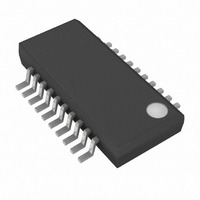
MAX1865TEEP+T Maxim Integrated Products, MAX1865TEEP+T Datasheet - Page 22

MAX1865TEEP+T
Manufacturer Part Number
MAX1865TEEP+T
Description
IC PWR SUPPLY CONTROLLER 20QSOP
Manufacturer
Maxim Integrated Products
Datasheet
1.MAX1864TEEE.pdf
(25 pages)
Specifications of MAX1865TEEP+T
Applications
Power Supply Controller
Voltage - Input
4.5 ~ 28 V
Current - Supply
1.4mA
Operating Temperature
-40°C ~ 85°C
Mounting Type
Surface Mount
Package / Case
20-QSOP
Lead Free Status / RoHS Status
Lead free / RoHS Compliant
Voltage - Supply
-
Lead Free Status / Rohs Status
Lead free / RoHS Compliant
xDSL/Cable Modem Triple/Quintuple Output
Power Supplies
only), connect the transformer as shown in Figure 6,
where the minimum turns ratio is determined by:
Since power transfer occurs when the low-side MOS-
FET is on (DL = high), the transformer cannot support
heavy loads with high duty cycles.
The MAX1864/MAX1865 use a current-mode control
scheme that senses the current across the high-side
MOSFET (N
has turned on, the MAX1864/MAX1865 use a 60ns cur-
rent-sense blanking period to minimize noise sensitivity.
When the MOSFET turns on, however, the transformer’s
secondary inductance and the diode’s parasitic capac-
itance form a resonant circuit that causes ringing.
Reflected back through the transformer to the primary
side, these oscillations across the high-side MOSFET
may last longer than the blanking period. A series RC
snubber circuit at the diode (Figure 6) increases the
damping factor, allowing the ringing to settle quickly.
Applications with multiple transformer windings require
only one snubber circuit on the highest output voltage.
Applications with low turn ratios (1:1), such as the
MAX1864 typical application circuit (Figure 1), may not
require a snubber curcuit.
The diode’s parasitic capacitance can be estimated
using the diode’s reverse voltage rating (V
capability (I
approximation is:
For the EC10QS10 Nihon diode used in figure 6, the
capacitance is roughly 15pF. The output snubber must
only dampen the ringing, so the initial turn-on spike that
occurs during the blanking period remains preset. A
100pF capacitor works well in most applications; larger
capacitance values require more charge, thereby
increasing the power dissipation.
The snubber’s time constant (t
than the 100ns blanking time. A typical RC time con-
stant of approximately 30ns was chosen for Figure 6:
22
______________________________________________________________________________________
N
NEG
R
SNUB
H
). Immediately after the high-side MOSFET
O
≥
C
), and recovery time (T
⎛
⎜ ⎜
⎝
DIODE
|
=
V
LDO NEG
C
t
SNUB
SNUB
(
=
I
O
V
)
=
RRM
×
|
V
+
C
t
OUT
RR
30
SNUB
V
SNUB
SAT
ns
+
) must be smaller
Snubber Design
V
DIODE
RR
RRM
). A rough
⎞
⎟ ⎟
⎠
), current
Under no-load conditions, leakage currents from the
pass transistors supply the output capacitor, even
when the transistor is off. Generally, this is not a prob-
lem since the feedback resistors’ current drains the
excess charge. However, charge may build up on the
output capacitor over temperature, making V
above its set point. Care must be taken to ensure that
the feedback resistors’ current exceeds the pass tran-
sistor’s leakage current over the entire temperature
range.
Careful PC board layout is critical to achieve low
switching losses and clean, stable operation. The
switching power stage requires particular attention.
Follow these guidelines for good PC board layout:
1) Place the power components first, with ground ter-
2) Mount the MAX1864/MAX1865 adjacent to the
3) Group the gate-drive components (BST diode and
4) All analog grounding must be done to a separate
Minimum Load Requirements (Linear Regulators)
minals adjacent (N
make all these connections on the top layer with
wide, copper-filled areas. Keep these high-current
paths short, especially at ground terminals.
switching MOSFETs to keep IN-LX current-sense
lines, LX-GND current-limit sense lines, and the dri-
ver lines (DL and DH) short and wide. The current-
sense amplifier inputs are connected between IN
and LX, so these pins must be connected as close
as possible to the high-side MOSFET. The current-
limit comparator inputs are connected between LX
and GND, but accuracy is not as important, so give
priority to the high-side MOSFET connections. The
IN, LX, and GND connections to the MOSFETs must
be made using Kelvin sense connections to guaran-
tee current-sense and current-limit accuracy.
capacitor, IN bypass capacitor) together near the
MAX1864/MAX1865.
solid copper ground plane, which connects to the
MAX1864/MAX1865 at the GND pin. This includes
the VL bypass capacitor, feedback resistors, com-
pensation components (R
adjustable current-limit threshold resistors connect-
ed to ILIM.
Applications Information
PC Board Layout Guidelines
L
source, C
COMP
IN
, C
OUT
, C
). If possible,
COMP
LDO
), and
rise


