SI8250-IQ Silicon Laboratories Inc, SI8250-IQ Datasheet
SI8250-IQ
Specifications of SI8250-IQ
Available stocks


Related parts for SI8250-IQ


SI8250-IQ Summary of contents
Page 1
... Onboard processing capability enables intelligent control optimization for improved system performance and new capabilities, such as serial connectivity via the SMBus or onboard UART. The Si8250/1/2 family is in-system Flash programmable, enabling control and protection parameters, such as system regulation and protection settings, startup and shutdown modes, loop response, and modulation timing readily modified ...
Page 2
... Si8250/1/2 2 Rev. 1.0 ...
Page 3
... System Management Processor Functional Block Descriptions . . . . . . . . . . . . . . . . 17 4. Design Tools . . . . . . . . . . . . . . . . . . . . . . . . . . . . . . . . . . . . . . . . . . . . . . . . . . . . . . . . . . . . 18 5. Example Applications . . . . . . . . . . . . . . . . . . . . . . . . . . . . . . . . . . . . . . . . . . . . . . . . . . . .19 5.1. Isolated DC/DC Converter . . . . . . . . . . . . . . . . . . . . . . . . . . . . . . . . . . . . . . . . . . . . 19 5.2. Single-Phase Point of Load (POL) Converter . . . . . . . . . . . . . . . . . . . . . . . . . . . . . . 20 6. Layout Considerations . . . . . . . . . . . . . . . . . . . . . . . . . . . . . . . . . . . . . . . . . . . . . . . . . . .21 7. Pin Descriptions: Si8250/1 7.1. Pin Functions . . . . . . . . . . . . . . . . . . . . . . . . . . . . . . . . . . . . . . . . . . . . . . . . . . . . . .24 8. Ordering Guide . . . . . . . . . . . . . . . . . . . . . . . . . . . . . . . . . . . . . . . . . . . . . . . . . . . . . . . . . . 25 9. Package Outline: 32LQFP . . . . . . . . . . . . . . . . . . . . . . . . . . . . . . . . . . . . . . . . . . . . . . . . . 26 10. Package Outline: 28QFN . . . . . . . . . . . . . . . . . . . . . . . . . . . . . . . . . . . . . . . . . . . . . . . . . 28 Document Change List . . . . . . . . . . . . . . . . . . . . . . . . . . . . . . . . . . . . . . . . . . . . . . . . . . . . .30 Contact Information ...
Page 4
... Si8250/1/2 1. Electrical Specifications Table 1. Absolute Maximum Ratings* Parameter Ambient temperature under bias Storage temperature Voltage on any Port0 Pin with respect to GND Voltage on all other pins with respect to GND Voltage on V with respect to GND DD Maximum total current through V DD Maximum output current sunk by RST or any port pin *Note: Stresses above those listed in this table may cause permanent device damage ...
Page 5
... Supply current Shutdown supply current Conditions Min — — –2 –1.0 1/2 LSB change from — full scale — 2 MHz BW — — — — Rev. 1.0 Si8250/1/2 Typ Max Units — 9 Bits 2.44 — mV — +2 LSB — +1.0 LSB 2 — µs 20 — ...
Page 6
... Si8250/1/2 Table 4. ADC0 (12-Bit ADC) Specifications T = –40 to +125 ° 2.5 V, SYSCLK = 25 MHz, PLLCLK = 200 MHz unless otherwise specified Parameter DC Accuracy Resolution Integral nonlinearity Differential nonlinearity Offset error Full scale error Offset temperature coefficient Dynamic Performance (10 kHz sine-wave Single-ended input below Full Scale, 200 ksps) ...
Page 7
... ADCSP2 = 1 ADCSP1 = 1 — 1.25 ADCSP2 = 1 — –32 0.8 –2 –1 — — — Disabled — — Conditions Min — — Disabled — Rev. 1.0 Si8250/1/2 Max Units 10 — 5 — Msps 2.5 — — — 6 Bits — — +31 LSB — 1.3 V — +2 LSB — ...
Page 8
... Si8250/1/2 Table 7. Peak Current Limit Detector Electrical Specifications T = –40 to +125 ° 2.5 V, SYSCLK = 25 MHz, PLLCLK = 200 MHz unless otherwise specified Parameter IPK input to DPWM output latency Threshold detector voltage Hysteresis Blanking time Input capacitance Input bias current Shutdown supply current Active supply current ...
Page 9
... OUT — OUT — Conditions Min — –1 (0.01%, 4.7 µF) — no load — 4.7 µF — — — — Rev. 1.0 Si8250/1/2 Typ Max Units — 200 — 50 MHz — 25 — 9 Bits — — — — — ns — ...
Page 10
... Si8250/1/2 Table 10. Comparator0 Specifications T = –40 to +125 ° 2.5 V, SYSCLK = 25 MHz, PLLCLK = 200 MHz unless otherwise specified Parameter V IN Low-speed supply current Full-speed supply current Hysteresis Low power mode overdrive Response time High-speed mode overdrive Input capacitance CMRR Input offset 10 Conditions Min 0 — ...
Page 11
... 0 RST = 0.0 Time from last system clock rising edge to start of reset tion at location 0x0000 100 Conditions Min Si8250 32768 Si8251, Si8252 16384 Rev. 1.0 Si8250/1/2 Typ Max Units — — 0.7 — — DD — — 0 — 2.0 2.1 2.2 — ...
Page 12
... Si8250/1/2 Table 13. Port I/O DC Electrical Characteristics T = –40 to +125 °C, SYSCLK = 25 MHz, PLLCLK = 200 MHz unless otherwise specified. A Parameters Port0 input voltage tolerance Port1 input voltage tolerance Output high voltage Output low voltage Input high voltage Input low voltage Input leakage current Table 14 ...
Page 13
... Temperature coefficient Supply current Shutdown current Conditions Min 24 — — — — — Conditions Min — — — — — — Rev. 1.0 Si8250/1/2 Typ Max Units 24.5 25 MHz 100 — µs 0.3 — %/V 50 — PPM/°C 450 — µA 0.1 — ...
Page 14
... The digital controller can be used to execute self-diagnostic routines during production test, thereby reducing test time and lowering cost. The small physical size of the Si8250 in particular ( mm) saves board space. Rev. 1.0 ...
Page 15
... VSENSE VSENSE ADC1 FILTER ENGINE 10Msps VREF REFDAC VREF Pulse-by-Pulse Current Limiter IPK and OCP Control Processor Figure 2. Si8250 Top-Level Block Diagram 4x 16-BIT TIMERS 16/32 kB SMBus Flash 3 CH PCA I/O PORT 1280 Byte LATCHES RAM UART VSENSE ADC 12-BIT ...
Page 16
... This signal connects to the pulse-by-pulse current-limiting hardware in the Si8250/1/2 via the IPK input pin. This current-limiting circuitry is similar to that found in a voltage mode analog PWM. It contains a fast analog comparator and a programmable leading-edge blanking ...
Page 17
... Temperature Sensor This sensor measures the die temperature of the Si8250/1/2. It can achieve 3 °C accuracy with a single- point calibration and 1 °C with a two-point calibration. The temperature output signal is digitized by ADC0. 3.3.3. 8051 CPU 50 MIPS CPU core with SRAM and Flash memory ...
Page 18
... Si8250/1/2 4. Design Tools The Si8250DK development kit (Figure 3) contains everything required to develop applications with the Si825x family of digital power controllers. This kit supports all phases of power supply development from controller design through real-time system debugging. It also includes a turnkey isolated dc/dc target board for evaluation and experimentation ...
Page 19
... Reference designs are available for both of these. For more details, visit our web site at www.silabs.com. 5.1. Isolated DC/DC Converter 400 kHz, Si8250-based half bridge converter is shown in Figure 7. This circuit is the same as that of the target (evaluation) board shipped in the Si8250DK development kit. ...
Page 20
... Si8250/1/2 5.2. Single-Phase Point of Load (POL) Converter 400 KHz Si8252 based single phase POL converter block diagram is shown in Figure 8. DPWM outputs PH1 and PH2 control the gates of the buck and synchronous switching transistors. A lossless current sensing method that relies on the resistor and inductance of the inductor is used to measure the current for overcurrent protection ...
Page 21
... Layout Considerations The mixed-signal nature of the Si8250/1/2 mandates clean bias supplies and ground returns best to provide separate ground planes for analog, digital, and power switch returns. These planes should tie together at only one point to eliminate the possibility of circulating ground currents. For best performance, the V should be decoupled from the main supply ...
Page 22
... Debug Pins (C2D, C2CK) Figure 12. Debug Interface Pin Protection Circuit best to locate the Si8250/1/2 as close to the output voltage terminal as possible and use a Kelvin connection to reduce the difference in ground potential between the Si8250/1/2 and the output voltage ground return. Most applications will require access to the debug pins ...
Page 23
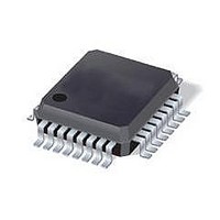
... Pin Descriptions: Si8250/1/2 32-pin LQFP RST/C2CK 1 IPK 2 VSENSE 3 Si8250/1/2 GNDA 4 Top View VDDA 5 6 VREF 7 P1.0/VIN/AIN0 8 P1.1/AIN1 Figure 13. Example Pin Configurations Name QFN-28 LQFP-32 Pin # Pin# RST/C2CK 1 IPK SENSE GND 4 GNDA — — DDA V 6 REF P1.0/V or AIN0 7 IN P1.1/AIN1 8 P1.2/AIN2 9 P1 ...
Page 24
... V SENSE ADC1 inverting input. This is the voltage feedback input for the Si8250. The maximum allowable signal is V 7.1.4. GND Digital ground for the 32LQFP package and the main ground for the 28MLP package. 7.1.5. GNDA Analog ground for 32LQFP only ...
Page 25
... Ordering Guide Ordering Number Flash Memory Si8250-IQ Si8250-IM Si8251-IQ Si8251-IM Si8252-IQ Si8252- PWM Outputs Rev. 1.0 Si8250/1/2 UART Package Yes LQFP-32 Yes QFN-28 Yes LQFP-32 Yes QFN-28 No LQFP-32 No QFN-28 25 ...
Page 26
... Si8250/1/2 9. Package Outline: 32LQFP Figure 14 illustrates the package details for the 32-pin LQFP version of the Si8250/1/2. Table 18 lists the values for the dimensions shown in the illustration. Figure 14. 32-pin LQFP Package Diagram 26 Rev. 1.0 ...
Page 27
... Recommended card reflow profile is per the JEDEC/IPC J-STD-020C 4. specification for small body components. Nom Max — 1.60 — 0.15 1.40 1.45 0.37 0.45 — 0.20 9.00 BSC. 7.00 BSC. 0.80 BSC. 9.00 BSC. 7.00 BSC. 0.60 0.75 0.20 0.20 0.10 0.20 3.5° 7° Rev. 1.0 Si8250/1/2 27 ...
Page 28
... Si8250/1/2 10. Package Outline: 28QFN Figure 15 illustrates the package details for the 28-lead QFN version of the Si8250/1/2. Table 19 lists the values for the dimensions shown in the illustration. Figure 15. 28-lead Quad Flat No-lead (QFN) Package Diagram 28 Rev. 1.0 ...
Page 29
... Recommended card reflow profile is per the JEDEC/IPC J-STD-020C specification for small body components. Nom Max 0.90 1.00 0.07 0.11 0.25 REF 0.25 0.30 5.00 BSC. 3.15 3.35 0.50 BSC. 5.00 BSC. 3.15 3.35 0.55 0.65 0.15 0.10 0.05 0.08 0.435 0.18 Rev. 1.0 Si8250/1/2 29 ...
Page 30
... Si8250/1 OCUMENT HANGE IST Revision 0.7 to Revision 0.8 Updated DPWM phase output drive-high and drive- low resistance in Table 8, “DPWM Specifications,” on page 9. Revision 0.8 to Revision 0.9 Updated Table 5, “ADC1 Specifications,” on page 7. Updated common-mode input voltage range spec. Updated "Contact Information" on page 32. ...
Page 31
... N : OTES Rev. 1.0 Si8250/1/2 31 ...
Page 32
... Si8250/1 ONTACT NFORMATION Silicon Laboratories Inc. 400 West Cesar Chavez Austin, TX 78701 Tel: 1+(512) 416-8500 Fax: 1+(512) 416-9669 Toll Free: 1+(877) 444-3032 Email: PowerProducts@silabs.com Internet: www.silabs.com The information in this document is believed to be accurate in all respects at the time of publication but is subject to change without notice. ...