IR3720MTRPBF International Rectifier, IR3720MTRPBF Datasheet
IR3720MTRPBF
Specifications of IR3720MTRPBF
Available stocks


Related parts for IR3720MTRPBF

IR3720MTRPBF Summary of contents
Page 1
... Phase R Single Phase Converter Power Return ORDERING INFORMATION Device IR3720MTRPBF * IR3720MPBF * Samples only Page DESCRIPTION The IR3720 measures the output voltage and inductor current of low-voltage DC-to-DC converters and reports the average power over a user specified time interval as a digital word on the I measured across a current sensing resistor or indirectly across the inductor’ ...
Page 2
ABSOLUTE MAXIMUM RATINGS All voltages referenced to GND VDD: ................................................................3.9V ALERT#:...........................................................3.9V ALERT#.............................................. <VDD + 0.3V EXTCLK ...........................................................3.9V All other Analog and Digital pins ......................3.9V Stresses beyond those listed under “Absolute Maximum Ratings” may cause permanent damage to the device. These ...
Page 3
PARAMETER DIGITIZER Internal Sampling frequency External Sampling frequency Transition time POWER INFORMATION Minimum Averaging Interval Maximum Averaging Interval Output Register Measuring power Output Register Measuring power Output Register Measuring power Output Register Measuring power Full Scale Output Register Measuring power ...
Page 4
SYSTEM ACCURACY TEST CIRCUIT VDD VDD VREF Bypass Cap R T Page DCR R CS2 C CS2 VCS VDD VO GND www.irf.com IR3720 DATA SHEET ALERT# VO EXTCLK ADDR SDA SCL 09/09/08 ...
Page 5
BLOCK DIAGRAM IC PIN DESCRIPTION NAME NUMBER I/O LEVEL VCS 1 Analog VO 2 Analog VREF 3 Analog GND 4 VDD 5 3.3V EXTCLK 6 3.3V Digital ADDR 7 3.3V Digital SCL 8 3.3V Digital SDA 9 3.3V Digital ALERT# ...
Page 6
IC PIN FUNCTIONS VDD PIN This pin provides operational bias current to circuits internal to the IR3720. Bypass it with a high quality ceramic capacitor to the GND pin. GND PIN This pin returns operational bias current to its source. ...
Page 7
TYPICAL PERFORMANCE CHARACTERISTICS (System Accuracy Test Circuit, VDD=3 Typical transfer characteristic - Power configuration Average of 8 samples 300 1.8V Ideal Code 0 -300 -0.035 0.000 V (V) DCR Typical ...
Page 8
... I through the inductor. Average power is measured with the aid of International Rectifier’s proprietary TruePower™ circuit. Voltage, current, or the product of voltage Vo and current is digitized over the interval of interest and ported to the OUTPUT register. The VCS pin is maintained at an average voltage equal to Vo ...
Page 9
RESISTOR SENSING APPLICATION The voltage on the shunt resistor of the circuit below is directly proportional to the current from the source. Shunts developing used. Accuracy is enhanced at the higher voltage. Select ...
Page 10
INDUCTOR DCR CURRENT SENSING APPLICATION Referring to the Functional Description Diagram, it can be seen that the shunt function can be accomplished by the DC resistance of the inductor that is already present. Omitting the resistive shunt reduces BOM cost ...
Page 11
THERMAL COMPENSATION FOR INDUCTOR DCR CURRENT SENSING The positive temperature coefficient of the DCR can be compensated if R varies inversely proportional to T the DCR. DCR of a copper coil function of temperature, is approximated by = ...
Page 12
TYPICAL 2-PHASE DCR-SENSING APPLICATION The IR3720 is capable of monitoring power in a multiphase converter. A two-phase circuit is shown below. The voltage output of any phase is equal to that of any and every other phase, and monitored at ...
Page 13
ERROR MANAGEMENT Component value errors external to the IR3720 contribute to power and current measurement error. The power reported by the IR3720 is a function not only of actual power or current, but also of products and quotients of R ...
Page 14
CONFIGURATION REGISTER A configuration register is maintained via the I MFR_SPECIFIC_00 command, code # D0h. The low order nibble (d3, d2, d1, d0) contains a binary number N from zero to eight. The averaging interval milliseconds. N ...
Page 15
OUTPUT REGISTER The output register is loaded with a two’s compliment factor of voltage, current, or power, depending on the last request loaded into the configuration register. I “Direct Data Format” is used. The value of the output register is ...
Page 16
PACKET PROTOCOL S = Start Condition W = Bus write (lo Bus read (hi Acknowledge for ACK, =1 for NACK P = Stop Condition = master to slave = slave to master Bus Write ...
Page 17
PCB PAD AND COMPONENT PLACEMENT The figure below shows suggested pad and component placement. Page www.irf.com 09/09/08 ...
Page 18
SOLDER RESIST The figure below shows the suggested solder resist placement. Page www.irf.com 09/09/08 ...
Page 19
STENCIL DESIGN The figure below shows a suggested stencil design. Page www.irf.com 09/09/08 ...
Page 20
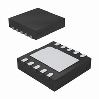
PACKAGE INFORMATION 3X3 MM 10L DFN LEAD FREE IR WORLD HEADQUARTERS: 233 Kansas St., El Segundo, California 90245, USA Tel: (310) 252-7105 Page Data and specifications subject to change without notice. This product has been designed and ...