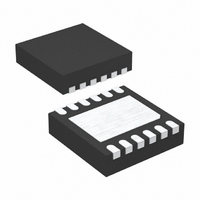
LTC2953IDD-1#PBF Linear Technology, LTC2953IDD-1#PBF Datasheet - Page 4

LTC2953IDD-1#PBF
Manufacturer Part Number
LTC2953IDD-1#PBF
Description
IC PB ON/OFF CONTROLLER 12DFN
Manufacturer
Linear Technology
Datasheet
1.LTC2953CDD-1PBF.pdf
(20 pages)
Specifications of LTC2953IDD-1#PBF
Applications
Push Button, On/Off Controller
Voltage - Supply
2.7 V ~ 27 V
Current - Supply
14µA
Operating Temperature
-40°C ~ 85°C
Mounting Type
Surface Mount
Package / Case
12-DFN
Ic Function
Push Button On/Off Controller With Voltage Monitoring
Supply Voltage Range
2.7V To 27V
Operating Temperature Range
-40°C To +85°C
Digital Ic Case Style
DFN
No. Of Pins
12
Svhc
No
Rohs Compliant
Yes
Lead Free Status / RoHS Status
Lead free / RoHS Compliant
Voltage - Input
-
Available stocks
Company
Part Number
Manufacturer
Quantity
Price
ELECTRICAL CHARACTERISTICS
LTC2953
SYMBOL
I
I
I
I
I
t
t
t
temperature range, otherwise specifi cations are at T
4
Note 1: Stresses beyond those listed under Absolute Maximum Ratings
may cause permanent damage to the device. Exposure to any Absolute
Maximum Rating condition for extended periods may affect device
reliability and lifetime.
Note 2: All currents into pins are positive; all voltages are referenced to
GND unless otherwise noted.
Note 3: The Enable Lock Out time is designed to allow an application to
properly power down such that the next power up sequence starts from a
consistent powered down confi guration. ⎯ P ⎯ B is ignored during this lock out
time. This time delay does not include t
PFI(LKG)
PFO(LKG)
UVLO(LKG)
VM(LKG)
RST(LKG)
PFI
RST
uv
PARAMETER
⎯ P ⎯ F ⎯ I Leakage Current
⎯ P ⎯ F O Leakage Current
UVLO Leakage Current
VM Input Leakage Current
⎯ R ⎯ S ⎯ T Output Leakage Current
⎯ P ⎯ F ⎯ I Delay to ⎯ P ⎯ F ⎯ O
Reset Timeout Period
VM Under Voltage Detect to ⎯ R ⎯ S ⎯ T
DB, ON
.
CONDITIONS
V
V
V
V
V
V
VM = 0.5V
V
VM Less Than VM
PFI
PFI
PFO
PFO
UVLO
UVLO
RST
= 0.5V
= 27V
A
= 1V
= 40V
= 3V
= 0.5V
= 27V
= 25°C. V
The
●
IN
(TH)
denotes the specifi cations which apply over the full operating
= 2.7V to 27V, unless otherwise noted (Note 2).
By More Than 1%
Note 4: To manually force a release of the EN/ ⎯ E ⎯ N pin, either ⎯ P ⎯ B or UVLO
must be held low for at least t
t
Note 5: The ⎯ K ⎯ I ⎯ L ⎯ L turn on blanking timer period (t
waiting period immediately after enable output is asserted. This blanking
time allows suffi cient time for the DC/DC converter and the μP to perform
power up tasks. The ⎯ K ⎯ I ⎯ L ⎯ L , ⎯ P ⎯ B and UVLO inputs are ignored during this
period. If ⎯ K ⎯ I ⎯ L ⎯ L remains low at the end of this blanking period, the enable
output is released, thus turning off system power.
PDT
(adjustable by placing external capacitor at PDT pin).
●
●
●
●
●
●
●
PD, Min
MIN
140
(internal default power down timer) +
40
TYP
100
200
250
2
2
2
2
KILL, ON BLANK
MAX
±0.1
±10
±10
±10
±10
200
260
±1
±1
±1
) is the
UNITS
2953f
ms
nA
μA
nA
μA
nA
μA
nA
μA
μs
μs


