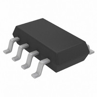
LTC2951CTS8-2#TRMPBF Linear Technology, LTC2951CTS8-2#TRMPBF Datasheet - Page 6

LTC2951CTS8-2#TRMPBF
Manufacturer Part Number
LTC2951CTS8-2#TRMPBF
Description
IC PB ON/OFF CONTROLLER TSOT23-8
Manufacturer
Linear Technology
Specifications of LTC2951CTS8-2#TRMPBF
Applications
Push Button, On/Off Controller
Voltage - Supply
2.7 V ~ 26.4 V
Current - Supply
6µA
Operating Temperature
0°C ~ 70°C
Mounting Type
Surface Mount
Package / Case
TSOT-23-8, TSOT-8
Operating Temperature (max)
70C
Operating Temperature (min)
0C
Pin Count
8
Mounting
Surface Mount
Package Type
TSOT-23
Case Length
2.9mm
Screening Level
Commercial
Lead Free Status / RoHS Status
Lead free / RoHS Compliant
Voltage - Input
-
Lead Free Status / Rohs Status
Compliant
Other names
LTC2951CTS8-2#TRMPBF
LTC2951CTS8-2#TRMPBFTR
LTC2951CTS8-2#TRMPBFTR
Available stocks
Company
Part Number
Manufacturer
Quantity
Price
PI FU CTIO S
LTC2951-1/LTC2951-2
6
V
⎯ P ⎯ B (Pin 2/Pin 3): Push Button Input. Connecting ⎯ P ⎯ B to
ground through a momentary switch provides on/off
control via the EN/ ⎯ E ⎯ N pin. An internal 100k pull-up resis-
tor connects to an internal 1.9V bias voltage. The rugged
⎯ P ⎯ B input can be pulled up to 26.4V externally without
consuming extra current.
KILLT (Pin 3/Pin 2): Additional, Adjustable ⎯ K ⎯ I ⎯ L ⎯ L Turn Off
Delay Input (t
ground provides additional delay time (beyond the internal
default 128ms, t
automatic release of the enable output. The ⎯ K ⎯ I ⎯ L ⎯ L turn off
delay feature ensures the release of the enable pin under
system fault conditions, such as the µP not responding
to the LTC2951 interrupt signal ( ⎯ I ⎯ N ⎯ T low).
GND (Pin 4/Pin 1): Device Ground.
⎯ I ⎯ N ⎯ T (Pin 5/Pin 8): Open Drain Interrupt Output. After a
push button turn-off event is detected (t
the LTC2951 interrupts the system (µP) by bringing the
⎯ I ⎯ N ⎯ T pin low. Once the system fi nishes its power down
and housekeeping tasks, it sets ⎯ K ⎯ I ⎯ L ⎯ L low, which in turn
releases the enable output. If at the end of the power
down timer period (t
DITIONAL
immediately. ⎯ I ⎯ N ⎯ T may optionally be tied to ⎯ K ⎯ I ⎯ L ⎯ L to release
the enable output immediately after the turn-off event has
been detected ( ⎯ I ⎯ N ⎯ T low).
EN (LTC2951-1, Pin 6/Pin 7): Open Drain Enable Output.
This pin is intended to enable system power. EN goes high
IN
U
(Pin 1/Pin 4): Power Supply Input: 2.7V to 26.4V.
) ⎯ K ⎯ I ⎯ L ⎯ L is still high, the enable output is released
U
⎯ K ⎯ I ⎯ L ⎯ L , OFF DELAY, ADDITIONAL
⎯ K ⎯ I ⎯ L ⎯ L , OFF DELAY
U
⎯ K ⎯ I ⎯ L ⎯ L , OFF DELAY
(TSOT-23/DFN)
) from ⎯ I ⎯ N ⎯ T falling to the
+ t
⎯ K ⎯ I ⎯ L ⎯ L , OFF DELAY, AD-
). A capacitor to
DB, OFF
+ t
OFFT
),
after a valid ⎯ P ⎯ B turn on event (t
⎯ K ⎯ I ⎯ L ⎯ L is not driven high within 512ms of the initial valid ⎯ P ⎯ B
power turn-on event, b) ⎯ K ⎯ I ⎯ L ⎯ L is driven low during normal
operation, or c) a second valid ⎯ P ⎯ B event (power turn-off)
is detected. The operating range for this pin is 0V to 10V.
A 100k pull-up is recommended if not available in the
DC/DC converter.
⎯ ⎯ E ⎯ N (LTC2951-2, Pin 6/Pin 7): Open Drain Enable Output.
This pin is intended to enable system power. ⎯ E ⎯ N is asserted
low after a valid ⎯ P ⎯ B turn-on event (t
high if: a) ⎯ K ⎯ I ⎯ L ⎯ L is not driven high within 512ms of the
initial valid ⎯ P ⎯ B power turn-on event, b) ⎯ K ⎯ I ⎯ L ⎯ L is driven low
during normal operation, or c) a second valid ⎯ P ⎯ B event
(power turn-off) is detected. The operating range of this
pin is 0V to 10V. A 100k pull-up is recommended if not
available in the DC/DC converter.
OFFT (Pin 7/Pin 6): Additional Adjustable Turn Off Time
Input (t
ditional time (beyond the internal default 32ms, t
that the ⎯ P ⎯ B pin must be held low before initiating a power
down sequence ( ⎯ I ⎯ N ⎯ T falling). Floating this pin results in a
default turn off debounce time of 32ms.
⎯ K ⎯ I ⎯ L ⎯ L (Pin 8/Pin 5): ⎯ K ⎯ I ⎯ L ⎯ L Input. Forcing ⎯ K ⎯ I ⎯ L ⎯ L low releases
the enable output. During system turn on, this pin is blanked
by a 512ms internal timer (t
system to pull ⎯ K ⎯ I ⎯ L ⎯ L high. This pin has an accurate 0.6V
threshold and can be used as a voltage monitor input.
Exposed Pad (Pin 9): Exposed Pad may be left open or
connected to device ground.
OFFT
). A capacitor to ground determines the ad-
⎯ K ⎯ I ⎯ L ⎯ L , ON BLANK
DB, ON
DB, ON
). EN goes low if: a)
). ⎯ E ⎯ N releases
) to allow the
DB, OFF
295112fa
)


