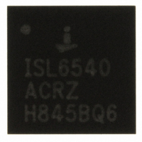
ISL6441IR Intersil, ISL6441IR Datasheet - Page 16

ISL6441IR
Manufacturer Part Number
ISL6441IR
Description
IC CTRLR SGL/STEP DOWN PWM 28QFN
Manufacturer
Intersil
Datasheet
1.ISL6441IRZ.pdf
(18 pages)
Specifications of ISL6441IR
Applications
Power Supplies
Current - Supply
2mA
Voltage - Supply
5.6 V ~ 24 V
Operating Temperature
-40°C ~ 85°C
Mounting Type
Surface Mount
Package / Case
28-QFN
Lead Free Status / RoHS Status
Contains lead / RoHS non-compliant
Available stocks
Company
Part Number
Manufacturer
Quantity
Price
Part Number:
ISL6441IR
Manufacturer:
INTERSIL
Quantity:
20 000
Company:
Part Number:
ISL6441IRZ
Manufacturer:
Intersil
Quantity:
600
Company:
Part Number:
ISL6441IRZ
Manufacturer:
IHTERSIL
Quantity:
2 500
Company:
Part Number:
ISL6441IRZ-TK
Manufacturer:
Intersil
Quantity:
2 400
The power dissipation includes two loss components;
conduction loss and switching loss. These losses are
distributed between the upper and lower MOSFETs
according to duty cycle (see Equations 10 and 11). The
conduction losses are the main component of power
dissipation for the lower MOSFETs. Only the upper MOSFET
has significant switching losses, since the lower device turns
on and off into near zero voltage. Equations 10 and 11
assume linear voltage-current transitions and do not model
power loss due to the reverse-recovery of the lower
MOSFET’s body diode.
A large gate-charge increases the switching time, t
which increases the upper MOSFET switching losses.
Ensure that both MOSFETs are within their maximum
junction temperature at high ambient temperature by
calculating the temperature rise according to package
thermal-resistance specifications.
Output Capacitor Selection
The output capacitors for each output have unique
requirements. In general, the output capacitors should be
selected to meet the dynamic regulation requirements
including ripple voltage and load transients. Selection of
output capacitors is also dependent on the output inductor,
so some inductor analysis is required to select the output
capacitors.
One of the parameters limiting the converter’s response to a
load transient is the time required for the inductor current to
slew to its new level. The ISL6441 will provide either 0% or
71% duty cycle in response to a load transient.
The response time is the time interval required to slew the
inductor current from an initial current value to the load
current level. During this interval the difference between the
inductor current and the transient current level must be
supplied by the output capacitor(s). Minimizing the response
time can minimize the output capacitance required. Also, if
the load transient rise time is slower than the inductor
response time, as in a hard drive or CD drive, it reduces the
requirement on the output capacitor.
The maximum capacitor value required to provide the full,
rising step, transient load current during the response time of
the inductor is shown in Equation 12:
where, C
output inductor, I
P
P
C
UPPER
LOWER
OUT
=
OUT
=
=
---------------------------------------------------------- -
2 V
(
(
-------------------------------------------------------------- -
(
------------------------------------------------------------------------------ -
I
I
O
(
O
IN
L
is the output capacitor(s) required, L
2
2
O
) r
–
) r
(
(
) I
TRAN
V
(
DS ON
DS ON
O
TRAN
) DV
V
(
(
(
IN
is the transient load current step, V
V
)
)
)
OUT
) V
IN
2
) V
(
(
OUT
IN
)
16
–
)
V
+
OUT
(
----------------------------------------------------------- -
I
O
)
) V
(
IN
) t
(
2
SW
) F
(
O
SW
SW
is the
(EQ. 10)
(EQ. 12)
(EQ. 11)
,
)
IN
ISL6441
is the input voltage, V
drop in output voltage allowed during the load transient.
High frequency capacitors initially supply the transient
current and slow the load rate-of-change seen by the bulk
capacitors. The bulk filter capacitor values are generally
determined by the ESR (Equivalent Series Resistance) and
voltage rating requirements as well as actual capacitance
requirements.
The output voltage ripple is due to the inductor ripple current
and the ESR of the output capacitors as defined by
where, I
page 17.
High frequency decoupling capacitors should be placed as
close to the power pins of the load as physically possible. Be
careful not to add inductance in the circuit board wiring that
could cancel the usefulness of these low inductance
components. Consult with the manufacturer of the load
circuitry for specific decoupling requirements.
Use only specialized low-ESR capacitors intended for
switching-regulator applications at 1.4MHz for the bulk
capacitors. In most cases, multiple small-case electrolytic
capacitors perform better than a single large-case capacitor.
The stability requirement on the selection of the output
capacitor is that the ‘ESR zero’, f
50kHz. This range is set by an internal, single compensation
zero at 10kHz. The ESR zero can be a factor of five on either
side of the internal zero and still contribute to increased
phase margin of the control loop. Therefore, see
Equation 14.
In conclusion, the output capacitors must meet three criteria:
The recommended output capacitor value for the ISL6441 is
between 150µF to 680µF, to meet stability criteria with
external compensation. Use of low ESR ceramic capacitors
is possible but would take more rigorous loop analysis to
ensure stability.
V
C
Equation 13.
1. They must have sufficient bulk capacitance to sustain the
2. The ESR must be sufficiently low to meet the desired
3. The ESR zero should be placed in a rather large range,
RIPPLE
OUT
output voltage during a load transient while the output
inductor current is slewing to the value of the load
transient,
output voltage ripple due to the output inductor current,
and
to provide additional phase margin.
=
L
----------------------------------- -
2π ESR
=
is calculated in the “Output Inductor Selection” on
(
ΔI
L
1
(
ESR
) f
( )
Z
)
O
is output voltage, and DV
Z
, be between 2kHz and
OUT
May 26, 2009
(EQ. 13)
(EQ. 14)
FN9197.3
is the


