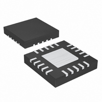
MAX1579ETG+ Maxim Integrated Products, MAX1579ETG+ Datasheet - Page 2

MAX1579ETG+
Manufacturer Part Number
MAX1579ETG+
Description
IC PS BIAS/WHITE LED TFT 24-TQFN
Manufacturer
Maxim Integrated Products
Datasheet
1.MAX1578ETGT.pdf
(13 pages)
Specifications of MAX1579ETG+
Applications
LCD Display
Current - Supply
3mA
Voltage - Supply
2.7 V ~ 5.5 V
Operating Temperature
-40°C ~ 85°C
Mounting Type
Surface Mount
Package / Case
24-TQFN Exposed Pad
Number Of Segments
8
Operating Supply Voltage
2.7 V to 5.5 V
Maximum Power Dissipation
1667 mW
Maximum Operating Temperature
+ 85 C
Mounting Style
SMD/SMT
Minimum Operating Temperature
- 40 C
Lead Free Status / RoHS Status
Lead free / RoHS Compliant
ABSOLUTE MAXIMUM RATINGS
IN, CS, C1N, C2N, MAIN, ONBIAS, V
CTRL to GND..................-0.3V to the lesser of +6V or (V
LX, OUT to GND .....................................................-0.3V to +37V
COMP to GND .............................................-0.3V to (V
CU1 to MAIN ............................................................-0.3V to +6V
CU2 to CU1 ..............................................................-0.3V to +6V
CU3 to CU2 ..............................................................-0.3V to +6V
CU3 to POS ............................................................-0.3V to +18V
CU3 to GND ...........................................................-0.3V to +18V
POS to GND ...........................................................-0.3V to +18V
CD1 to MAIN ..........................................................+0.3V to -12V
CD1 to GND .............................................................+0.3V to -6V
CD2 to CD1 ..............................................................+0.3V to -6V
NEG to CD2..............................................................+0.3V to -6V
Complete Bias and White LED Power Supplies
for Small TFT Displays
ELECTRICAL CHARACTERISTICS
(Circuit of Figure 3, V
Stresses beyond those listed under “Absolute Maximum Ratings” may cause permanent damage to the device. These are stress ratings only, and functional
operation of the device at these or any other conditions beyond those indicated in the operational sections of the specifications is not implied. Exposure to
absolute maximum rating conditions for extended periods may affect device reliability.
2
IN Operating Supply Range
IN Undervoltage-Lockout (UVLO)
Threshold
IN Quiescent Current
IN Shutdown Current
Thermal Shutdown
MAIN CHARGE PUMP WITH LINEAR REGULATOR
Main Pump Efficiency
V
Output Impedance
Operating Frequency
V
V
V
Quiescent Current
(Charge Pumps Only)
V
Discharge Switch Resistance
at V
POS, NEG CHARGE PUMPS
Operating Frequency
Duty Cycle
POS Pump Efficiency
POS Output Voltage
P OS D i schar g e S w i tch Resi stance
NEG Pump Efficiency
DD
DD
IN
IN
MAIN
_______________________________________________________________________________________
Fal l i ng S w i tchover to 2.0x M od e
Ri si ng S w i tchover to 1.5x M od e
MAIN
Charge-Pump Open-Loop
Output Voltage
Regulation Voltage
PARAMETER
IN
= 3V, CTRL = ONBIAS = IN, T
Rising edge, 30mV hysteresis
Switching
V
Rising temperature, 20°C hysteresis (typ)
I
V
V
Charge-pump pause threshold
V
0.1mA < I
V
I
I
V
I
DD
LOAD
LOAD
LOAD
LOAD
CTRL
IN
IN
CTRL
ONBIAS
ONBIAS
to GND.....-0.3V to +6V
≥ 3.8V in 1.5x mode
≥ 3.0V in 2.0x mode
= 25mA, V
= 100µA
= 0 to 100µA
= -100µA
= V
= 0V, ONBIAS = IN
= 0V
= 0V
LOAD
ONBIAS
A
< 25mA
= -40°C to +85°C, typical values are at T
IN
IN
= 0V
IN
+ 0.3V)
= 3.9V
+ 2V)
CONDITIONS
NEG, CD2 to GND..................................................+0.3V to -12V
C1P, C2P to GND ...........................................-0.3V to (V
PMP, PMPB to GND ................................-0.3V to (V
GND to PGND .......................................................-0.3V to +0.3V
I
Continuous Power Dissipation (T
Short-Circuit Duration (MAIN, POS, NEG)..................Continuous
Operating Temperature Range ...........................-40°C to +85°C
Junction Temperature ......................................................+150°C
Storage Temperature Range .............................-65°C to +150°C
Lead Temperature (soldering, 10s) ................................ +300°C
LX
(derate 20.8mW/°C above +70°C) .............................1667mW
24-Pin 4mm x 4mm Thin QFN
...................................................................................1.0A
T
T
A
A
= +25°C
= +85°C
A
= +25°C, unless otherwise noted. Note 1)
3.75
12.0
13.9
MIN
200
2.7
2.1
5.2
3.8
4.9
A
= +70°C)
+160
TYP
2.35
3.85
0.87
15.6
14.7
250
0.4
7.5
5.5
3.9
5.0
83
50
97
97
3
1
9
1
3
MAX
3.95
1.30
19.5
15.3
300
5.5
2.6
5.7
4.0
5.1
20
20
5
1
3
6
MAIN
IN
UNITS
+ 0.3V)
kHz
kHz
mA
mA
kΩ
kΩ
µA
°C
%
%
%
%
+ 6V)
Ω
V
V
V
V
V
V
V
RMS


