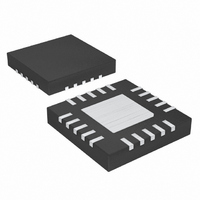
MAX17000AETG+T Maxim Integrated Products, MAX17000AETG+T Datasheet - Page 13

MAX17000AETG+T
Manufacturer Part Number
MAX17000AETG+T
Description
IC PWM CTLR DDR/DDR2/DDR3 24TQFN
Manufacturer
Maxim Integrated Products
Series
Quick-PWM™r
Datasheet
1.MAX17000ETG.pdf
(32 pages)
Specifications of MAX17000AETG+T
Applications
Memory, DDR2/DDR3 Regulator
Current - Supply
2mA
Voltage - Supply
4.5 V ~ 5.5 V
Operating Temperature
-40°C ~ 85°C
Mounting Type
Surface Mount
Package / Case
24-TQFN Exposed Pad
Lead Free Status / RoHS Status
Lead free / RoHS Compliant
PIN
14
15
16
17
18
19
20
21
22
23
24
—
PGND1
NAME
AGND
SHDN
SKIP
TON
BST
V
V
DH
______________________________________________________________________________________
LX
DL
EP
DD
CC
Switching Frequency Setting Input. An external resistor between the input power source and this
pin sets the switching frequency per phase according to the following equation:
High-Side Gate-Driver Output. Swings from LX to BST. DH is low when in shutdown or UVLO.
Inductor Connection. Connect LX to the switched side of the inductor as shown in Figure 1.
Boost Flying Capacitor Connection. Connect to an external 0.1µF, 6V capacitor as shown in Figure
1. The MAX17000 contains an internal boost switch.
Synchronous-Rectifier Gate-Driver Output. DL swings from V
Supply Voltage Input for the DL Gate Driver and 3.3V Reference/Analog Supply. Connect to the
system supply voltage (+4.5V to +5.5V). Bypass V
ceramic capacitor.
Power Ground. Ground connection for the low-side MOSFET gate driver.
Analog Ground. Connect backside exposed pad to AGND.
Pulse-skipping Control Input. This input determines the mode of operation under normal steady-
state conditions and dynamic output voltage transitions:
Controller Supply Voltage. Connect to a 4.5V to 5.5V source. Bypass V
greater ceramic capacitor.
Shutdown Control Input. Connect to V
MAX17000 slowly ramps down the output voltage to ground. When the internal target voltage
reaches 25mV, the controller forces DL low, and enters the low current (1µA) shutdown state.
When discharge mode is enabled by OVP (OVP = high), the CSL and VTT internal 16
MOSFETs are enabled in shutdown. When discharge mode is disabled by OVP (OVP = low), LX,
VTT, and VTTR are high impedance in shutdown.
A rising edge on SHDN clears the fault OV protection latch.
Exposed Pad. Connect backside exposed pad to AGND.
T
where C
TON is high impedance in shutdown.
High (> 2.4V) = Forced-PWM operation
Low (AGND) = Pulse-skipping mode
SW
Complete DDR2 and DDR3 Memory
= C
TON
TON
= 16.26pF.
x (R
TON
Power-Management Solution
+ 6.5k )
CC
for normal operation. When SHDN is pulled low, the
FUNCTION
DD
Pin Description (continued)
to power ground with a 1µF or greater
DD
to PGND1.
CC
to AGND with a 1µF or
discharge
13


