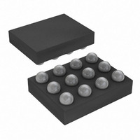
MAX14530EWC+T Maxim Integrated Products, MAX14530EWC+T Datasheet - Page 7

MAX14530EWC+T
Manufacturer Part Number
MAX14530EWC+T
Description
IC OVERVOLT PROT 6.8V 12-WLP
Manufacturer
Maxim Integrated Products
Datasheet
1.MAX14529EWCT.pdf
(9 pages)
Specifications of MAX14530EWC+T
Applications
Overvoltage Protection
Voltage - Supply
2.2 V ~ 28 V
Operating Temperature
-40°C ~ 85°C
Mounting Type
Surface Mount
Package / Case
12-WLP
Lead Free Status / RoHS Status
Lead free / RoHS Compliant
Current - Supply
-
Lead Free Status / Rohs Status
Lead free / RoHS Compliant
The MAX14529E/MAX14530E have an internal oscillator
and charge pump that control the turn-on of the internal
FET switch. The internal oscillator controls the timers
that enable the turn-on of the charge pump and con-
trols the state of the open-drain VOK output. If V
V
the charge pump. If 2.2V < V
charge pump is enabled. The charge-pump turns on
the internal FET switch and asserts VOK. At any time, if
V
high and the charge pump is disabled, disconnecting
OUT from IN.
The MAX14529E has a 5.75V (typ) overvoltage
threshold (OVLO), while the MAX14530E has a 6.8V
(typ) OVLO.
The low-dropout regulator (LOUT) is powered from
input voltage and supplies 3.3V (typ) to the USB trans-
ceiver. If a lithium-ion (Li+) battery is used to power the
USB transceiver, a boost converter is needed. The LDO
features a minimum 100mA current capability and low
output noise. Drive LEN high to disable the LDO.
The charger detection detects if there is a short
between the USB D+ and D- data lines. If the data lines
are shorted together and a dedicated charger is
attached, the phone draws more than 500mA to charge
the battery; CDET asserts low. If the data lines are not
biased properly, then an unidentified device is present
and the phone draws no more than 500mA or does not
charge at all, depending on its USB compliance level.
The MAX14529E/MAX14530E feature thermal-
shutdown circuitry. The internal switch turns off when
the junction temperature exceeds +150°C (typ) and
immediately goes into a fault mode. The device exits
thermal shutdown after the junction temperature cools
by 20°C (typ).
Bypass IN to GND with a 1µF ceramic capacitor as
close as possible to the device for ±15kV HBM ESD
protection on IN. No capacitor required to obtain ±2kV
HBM protection. If the power source has significant
OVLO
IN
drops below 2.2V or rises above V
, the internal oscillator remains off, thus disabling
Detection, LDO, and ESD Protection on D+/D-
Overvoltage Protection with USB Charger
Applications Information
Thermal-Shutdown Protection
_______________________________________________________________________________________
Overvoltage Lockout (OVLO)
IN Bypass Capacitor
IN
Charger Detection
Device Operation
< V
OVLO
OVLO
Low Dropout
, the internal
, VOK goes
IN
>
inductance due to long lead length, take care to
prevent overshoots due to the LC tank circuit and pro-
vide protection.
ESD performance depends on a number of conditions.
The MAX14529E/MAX14530E are specified for
±15kV HBM typical ESD protection on the D+, D-, and
IN pins when IN is bypassed to ground with a 1µF
ceramic capacitor.
Figure 2 shows the Human Body Model, and Figure 3
shows the current waveform it generates when dis-
charged into a low impedance. This model consists of
a 100pF capacitor charged to the ESD voltage of inter-
est that is then discharged into the device through a
1.5kΩ resistor.
Figure 2. Human Body ESD Test Model
Figure 3. Human Body Current Waveform
AMPERES
VOLTAGE
SOURCE
HIGH-
DC
I
P
36.8%
100%
90%
10%
CHARGE-CURRENT-
0
LIMIT RESISTOR
0
1MΩ
t
RL
R
100pF
C
C s
STORAGE
CAPACITOR
CURRENT WAVEFORM
TIME
RESISTANCE
1500Ω
DISCHARGE
R
D
ESD Test Conditions
t
DL
Human Body Model
I R
PEAK-TO-PEAK RINGING
(NOT DRAWN TO SCALE)
DEVICE
UNDER
TEST
7


