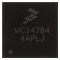
MC34704AEP Freescale Semiconductor, MC34704AEP Datasheet - Page 40

MC34704AEP
Manufacturer Part Number
MC34704AEP
Description
IC POWER MANAGEMENT 56-QFN
Manufacturer
Freescale Semiconductor
Datasheet
1.MC34704BEPR2.pdf
(54 pages)
Specifications of MC34704AEP
Applications
Processor
Current - Supply
86mA
Voltage - Supply
2.7 V ~ 5.5 V
Operating Temperature
-20°C ~ 85°C
Mounting Type
Surface Mount
Package / Case
56-QFN
Output Voltage
5 V
Input Voltage
2.7 V to 5.5 V
Switching Frequency
750 KHz to 2 MHz
Mounting Style
SMD/SMT
Number Of Outputs
8
Lead Free Status / RoHS Status
Lead free / RoHS Compliant
inductor rated between 50 to 100 mA in order to have this
regulator working in DCM. Rising the inductor value will make
the regulator to begin working in CCM.
• C
• 1CVG (Only Reg1): Use a 47uF capacitor from Ground to
• D1 (Only Reg1): Use a fast recovery schottky diode rated
Regulator 2, 4 and 5 (Synchronous Buck-Boost regulator
with external compensation)
boost voltage mode control DC-DC regulator that can
operate at various output voltage levels. Since each of the
40
34704
FUNCTIONAL DEVICE OPERATION
COMPONENT CALCULATION
C
ESR
L
L
1. Define I
2. However the worst case condition for the boost power
Note: On the 34704B Use the recommended 3.0uH
contribute to its impedance and output voltage ripple are
the ESR, the ESL and the capacitance C. The minimum
capacitor value is approximately:
• Where
• Now calculate the maximum allowed ESR to reach the
VG.
to 10V at 1A.
These three regulators are 4-Switch synchronous buck-
min
OUT
min
OUT
15% of full load.
stage is when the input voltage is equal to one half of
the output voltage, which results in the Maximum
then:
desired
where: D = Dutycycle
≥
≥
≤
where: Dmax = Maximum Dutycycle
≥
: The three elements of output capacitor that
Vo D
------------------------------------------ -
Vo T ( )
--------------- -
-------------------------------------------- -
⎛
⎝
16I
Io
---------------------------- -
-----------------------
1
FswΔVo
Vo = Output Voltage
T = Switching Period
IOB = Boundary Current to achieve CCM
Io
max
–
( ) 1
OB
FSW = Switching Frequency
Δ
OB
Δ
D
max
VO
2I
ΔVo
VO
max
(
D
as the minimum current to maintain CCM as
OB
max
r
–
r
is the desired output voltage ripple.
.
r
r
+
D
I
)
OB
2
T
⎞
⎠
[Ω]
(H)
(H)
(F)
Δ
I
L
,
regulators may work as a buck or a boost depending on the
operating voltages, they need to be compensated in different
ways for each situation.
operating input voltage range is set from 2.7 - 4.2 V, then the
following scenarios are possible:
• NOTE: Since these 3 regulators can work as a buck or a
Compensating for Buck operation:
• L: A buck power stage can be designed to operate in CCM
• C
where: RDSONLSFET = Body Resistance of the Lowside Fet
L
1. Define I
min
Since the 34704 is meant to work using a LiIon battery, the
boost in a single application, a good practice to configure
these regulators is to compensate for a boost scenario and
then verify that the regulator is working in buck mode using
that same compensation.
for load currents above a certain level usually 5 to 15% of
full load. The minimum value of inductor to maintain CCM
can be determined by using the following procedure:
contribute to its impedance and output voltage ripple are
the ESR, the ESL and the capacitance C. A good
approach to calculate the minimum real capacitance
needed is to include the transient response analysis to
control the maximum overshoot as desired.
OUT
15% of full load.
Regulator
≥
RL = Inductor Winding Resistance
D'Min = Minimum Off Percentage given by 1- (Vin_min/Vout_max)
D'max = Maximum Off Percentage given by 1- (Vin_max/Vout_min)
(
-------------------------------------------------------------------------------------------------------------------------- -
Vo
: The three elements of output capacitor that
2
4
5
+
Io
OB
max
as the minimum current to maintain CCM as
(
R
DSONLSFET
2.8 V
3.3 V
3.3 V
1.8 V
2.5 V
3.3 V
3.3 V
Vo
Analog Integrated Circuit Device Data
2I
OB
Input voltage
+
R
3.0 - 4.2
2.7 - 3.0
3.5 - 4.2
2.7 - 4.2
2.7 - 4.2
2.7 - 3.0
3.5 - 4.2
Freescale Semiconductor
L
range
)D′
min
)T
≈
D′
MAX
Operation
Boost
Boost
Buck
Buck
Buck
Buck
Buck
T
--------------
2I
[H]
Vo
OB


