ISL97645IRZ-T Intersil, ISL97645IRZ-T Datasheet
ISL97645IRZ-T
Specifications of ISL97645IRZ-T


Related parts for ISL97645IRZ-T

ISL97645IRZ-T Summary of contents
Page 1
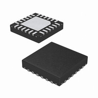
... All other trademarks mentioned are the property of their respective owners. ISL97645A FN6353.1 VDD Slice ON S ISL97645A (24 LD 4x4 QFN) TOP VIEW VIN2 2 17 FREQ2 3 16 COMP RESET Intersil (and design registered trademark of Intersil Americas Inc. Copyright Intersil Americas Inc. 2007, 2010. All Rights Reserved ...
Page 2
Pin Descriptions PIN NUMBER NAME 1 GND Signal ground 2 VGH_M Gate Pulse Modulator Output 3 VFLK Gate Pulse Modulator Control input 4 VDPM Gate Pulse Modulator Enable. Connect a capacitor from VDPM to GND to set the delay time ...
Page 3
... Storage Temperature . . . . . . . . . . . . . . . . . . . . . . . .-65°C to +150°C Maximum Continuous Junction Temperature . . . . . . . . . . . +125°C Power Dissipation ≤ +25° .2.44W +70° .1.34W +85° .0.98W +100° .0.61W A Pb-Free Reflow Profile http://www.intersil.com/pbfree/Pb-FreeReflow.asp = V = 14V 25V, AV DD1 DD2 GH TEST CONDITION ENABLE = 0V ENABLE = 5V, LX not switching V Rising IN2 V Falling IN2 ...
Page 4
Electrical Specifications V = ENABLE = 5V Unless Otherwise Noted. Boldface limits apply over the operating temperature range, -40°C to +85°C. (Continued) SYMBOL PARAMETER I FB Input Bias Current FB r Switch ON-resistance DS(ON) EFF Peak Efficiency I ...
Page 5
Electrical Specifications V = ENABLE = 5V Unless Otherwise Noted. Boldface limits apply over the operating temperature range, -40°C to +85°C. (Continued) SYMBOL PARAMETER SUPPLY MONITOR V VDIV High Threshold IH_VDIV V VDIV Low Threshold IL_VDIV I CD2 ...
Page 6
Typical Performance Curves CE = 1pF 100k VGH_M VFLK FIGURE 5. GPM CIRCUIT WAVEFORM CE = 10pF 100k VGH_M VFLK FIGURE 7. GPM CIRCUIT WAVEFORM FIGURE 9. V FOLLOWS V WHEN THE SYSTEM GHM GH POWERS ...
Page 7
Typical Performance Curves 7 ISL97645A (Continued) INPUT SIGNAL OUTPUT SIGNAL (-3dB ATTENTUATION FROM INPUT SIGNAL) FIGURE 11. V BANDWIDTH MEASUREMENT COM FN6353.1 October 21, 2010 ...
Page 8
Block Diagram FREQ OSCILLATION GENERATOR SLOPE COMPENSATION COMP - FB + REFERENCE GENERATOR FAULT CONTROL ENABLE 10µA CD2 + - V REF RESET VDIV + - V REF 750Ω VFLK VGH 8 ISL97645A SUMMING AMPLIFIER START-UP AND + - GPM ...
Page 9
Functional Block Diagram V IN VIN COMP SS VSHDN FREQ- VDPM VFLK CE RE POS NEG- VIN RESET AGND GND Applications Information The ISL97645A provides a complete power solution for TFT LCD applications. The system consists of one boost converter ...
Page 10
Operation The boost converter is a current mode PWM converter operating at either a 650kHz or 1.2MHz. It can operate in both discontinuous conduction mode (DCM) at light load and continuous mode (CCM). In continuous current mode, current flows continuously ...
Page 11
... Fairchild Semiconductor International Rectifier Vishay Semiconductor FIGURE 14. CASCADED MOSFET TOPOLOGY FOR HIGH 1 O × --- - (EQ the equation above assumes the OUT SIZE MFG PART NUMBER 1210 TDK C3225X7R1E106M 1210 Murata GRM32DR61E106K . VDD LX FB INTERSIL ISL97645A OUTPUT VOLTAGE APPLICATIONS October 21, 2010 A VDD FN6353.1 ...
Page 12
Supply Monitor Circuit The Supply Monitor circuit monitors the voltage on VDIV, and sets open-drain output RESET low when VDIV is below 1.15V (rising) or 1.1V (falling). There is a delay on the rising edge, controlled by a capacitor on ...
Page 13
VGH_M VGH_M VDD1 RE CE VFLK FIGURE 16. GATE PULSE MODULATOR CIRCUIT BLOCK DIAGRAM hreshold ...
Page 14
V VDPM >VLOR <1.215V x <1.215V >VLOR >1.215V x x Start-Up Sequence When V exceeds VLOR and ENABLE reaches the VIH IN threshold value, Boost converter starts up, and gate pulse modulator circuit output holds until VDPM ...
Page 15
... Accordingly, the reader is cautioned to verify that data sheets are current before placing orders. Information furnished by Intersil is believed to be accurate and reliable. However, no responsibility is assumed by Intersil or its subsidiaries for its use; nor for any infringements of patents or other rights of third parties which may result from its use ...
Page 16
Package Outline Drawing L24.4x4D 24 LEAD QUAD FLAT NO-LEAD PLASTIC PACKAGE Rev 2, 10/06 4.00 PIN 1 INDEX AREA (4X) 0.15 TOP VIEW ( TYP ) ( TYPICAL RECOMMENDED LAND PATTERN 16 ISL97645A ...