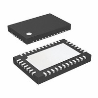
ISL97522IRZ-T Intersil, ISL97522IRZ-T Datasheet - Page 18

ISL97522IRZ-T
Manufacturer Part Number
ISL97522IRZ-T
Description
IC SUPPLY CTRL 4CH TFT-LCD 38QFN
Manufacturer
Intersil
Datasheet
1.ISL97522IRZ-T.pdf
(20 pages)
Specifications of ISL97522IRZ-T
Applications
LCD TV/Monitor
Current - Supply
3mA
Voltage - Supply
4.5 V ~ 13.2 V
Operating Temperature
-40°C ~ 85°C
Mounting Type
Surface Mount
Package / Case
38-QFN
Lead Free Status / RoHS Status
Lead free / RoHS Compliant
Fault Protection
During the startup sequence, prior to BOOST soft-start,
V
device temperature is checked. If either of these are not
within the expected range, the part is disabled until the
power is recycled or EN is toggled.
If C
while if C
occur and the sequence will not complete.
Once the start-up sequence is completed, the chip
continuously monitors C
and FBB for faults. During this time, the voltage on the C
capacitor remains at 1.15V until either a fault is detected, or
the EN pin is pulled low.
A fault on C
chip immediately. If a fault on any other output is detected,
C
the upper fault threshold (typically 2.4V), at which point the
chip is disabled until the power is recycled or EN is toggled.
If the fault condition is removed prior to the end of the ramp,
the voltage on the C
Typical fault thresholds for FBP, FBL, FBN and FBB are
included in the tables. DELB fault threshold is typically 0.6V.
C
keep the voltage within their normal ranges. If they are
shorted low, the regulators will attempt to regulate to 0V.
If any of the regulated outputs (AVDD, V
V
circuitry will switch off until the output returns to its expected
value.
If AVDD and V
limit will prevent damage to the chip. While in current limit,
the part acts like a current source and the regulated output
will drop. If the output drops below the fault threshold, a
ramp will be initiated on C
is sustained, the chip will be disabled on completion of the
ramp.
In some circumstances, (depending on ambient temperature
and thermal design of the board), continuous operation at
current limit may result in the over-temperature threshold
being exceeded, which will cause the part to disable
immediately.
All I/O also have ESD protection, which in many cases will
also provide overvoltage protection, relative to either ground
or V
abs max ratings are exceeded.
REF
DELAY
INTB
LOGIC
DELAY
DD
is checked to be within ±20% of its final value and the
and C
. However, these will not generally operate unless
) are driven above their target levels the drive
will ramp up linearly with a 5µA (typical) current to
DELAY
is shorted low, then the sequence will not start,
DELAY
INTL
LOGIC
is shorted H, the first down ramp will not
have an internal current-limited clamp to
, V
DLY
REF
are excessively loaded, the current
DLY
capacitor returns to 1.15V.
or temperature will shut down the
DELAY
, DELB, FBP, FBL, FBN, V
18
and, provided that the fault
ON
, V
OFF
or
REF
DLY
ISL97522
Component Selection for Start-Up Sequencing and
Fault Protection
The C
to stabilize the V
22nF to 1µF and should not be more than five times the
capacitor on C
The C
range from 47nF minimum to several microfarads - only
limited by the leakage in the capacitor reaching µA levels.
C
above). Note with 220nF on C
typically 50ms and the use of a larger/smaller value will vary
this time proportionally (e.g. 1µF will give a fault time-out
period of typically 230ms).
Fault Sequencing
The ISL97522 has an advanced fault detection system
which protects the IC from both adjacent pin shorts during
operation and shorts on the output supplies.
A high quality layout/design of the PCB, in respect of
grounding quality and decoupling is necessary to avoid
falsely triggering the fault detection scheme - especially
during start-up. The user is directed to the layout guidelines
and component selection sections to avoid problems during
initial evaluation and prototype PCB generation.
Over-Temperature Protection
An internal temperature sensor continuously monitors the
die temperature. In the event that the die temperature
exceeds the thermal trip point of 140°C, the device will shut
down.
Layout Recommendation
The device's performance including efficiency, output noise,
transient response and control loop stability is dramatically
affected by the PCB layout. PCB layout is critical, especially
at high switching frequency.
There are some general guidelines for layout:
1. Place the external power components (the input
2. Place V
3. Minimize the length of traces carrying fast signals and
4. All feedback networks should sense the output voltage
5. The power ground (PGND) and signal ground (SGND)
DEL
capacitors, output capacitors, boost inductor and output
diodes, etc.) in close proximity to the device. Traces to
these components should be kept as short and wide as
possible to minimize parasitic inductance and resistance.
the pins.
high current.
directly from the point of load, and be as far away from LX
node as possible.
pins should be connected at only one point near the main
decoupling capacitors.
REF
DEL
should be at least 1/5 of the value of C
capacitor is typically 220nF and has a usable
capacitor is typically set at 220nF and is required
REF
DEL
, V
REF
DC
to ensure correct start-up operation.
output. The range of C
and V
DCP
DEL
bypass capacitors close to
the fault time-out will be
REF
REF
December 13, 2006
is from
(See
FN7445.0


