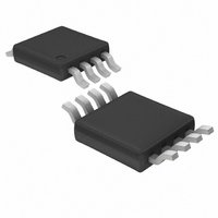
LTC1699EMS8-81#TR Linear Technology, LTC1699EMS8-81#TR Datasheet - Page 6

LTC1699EMS8-81#TR
Manufacturer Part Number
LTC1699EMS8-81#TR
Description
IC PROGRAMMER VOLT SMBUS 8MSOP
Manufacturer
Linear Technology
Datasheet
1.LTC1699EMS8-82.pdf
(20 pages)
Specifications of LTC1699EMS8-81#TR
Applications
Processor
Current - Supply
350µA
Voltage - Supply
2.7 V ~ 5.5 V
Operating Temperature
-40°C ~ 85°C
Mounting Type
Surface Mount
Package / Case
8-MSOP, Micro8™, 8-uMAX, 8-uSOP,
Lead Free Status / RoHS Status
Contains lead / RoHS non-compliant
Available stocks
Company
Part Number
Manufacturer
Quantity
Price
LTC1699 Series
PI FU CTIO S
Note: Pin numbers apply to 16-lead SSOP packages.
SEL (Pin 1): Register Select Input. A TTL compatible logic
input pin that is used to select 1 of 2 resistor divider
settings. SEL selects the setting in Register 0 if pulled low
and the setting in Register 1 if pulled high.
NC (Pin 2): Not connected.
SDA (Pin 3): SMBus Data Input/Output. SDA is a high
impedance input when address, command or data bits are
shifted in. It is an open drain, N-channel output when
acknowledging or sending data back to the microproces-
sor during read-back. It requires a pull-up resistor or
current source to V
SCL (Pin 4): SMBus Clock Input. Data at the SDA pin is
latched into the LTC1699 at the rising edge of the clock and
is shifted out of the SDA pin at the falling edge of the clock.
SCL is a high impedance input pin. It is driven by the open
collector output of a microprocessor and requires a pull-
up resistor or current source to V
VRON (Pin 5): Global Control Input. This TTL compatible
input pin is pulled up internally by a 2.5 A current source.
Pulling VRON low forces the open drain output pins
(CPU_ON, IO_ON, CLK_ON and PGOOD) to pull to ground.
If the LTC1699-80, LTC1699-81 or LTC1699-82 is pro-
grammed to turn on DC/DC converters, pulling VRON high
three-states the CPU_ON, IO_ON and CLK_ON pins and
allows the DC/DC converters to soft-start.
PGOOD (Pin 6): Power Good Output. This open drain
output is pulled low for 50 s each time the LTC1699-80,
LTC1699-81 or LTC1699-82 turns on the DC/DC convert-
ers or SEL is toggled to select a new code. PGOOD may be
connected to the FCB input of an LTC DC/DC converter to
force the converter into continuous mode operation. This
reduces the time needed for the converter output to settle
to a lower output voltage under light load conditions if the
SEL pin is toggled.
6
U
U
CC
U
.
CC
.
NC (Pin 7): Not connected.
CPU_ON (Pin 8): CPU DC/DC Converter Control. Open
drain output, usually connected to the RUN/SS pin of a DC/
DC converter that generates the CPU core supply. It pulls
low to shut down the converter or becomes a high imped-
ance state to allow the converter to soft-start.
IO_ON (Pin 9): I/O DC/DC Converter Control. Open drain
output, normally connected to the RUN/SS pin of the DC/
DC converter that generates the I/O supply. It pulls low to
shut down the converter or becomes a high impedance
state to allow the converter to soft-start.
CLK_ON (Pin 10): Clock DC/DC Converter Control. Open
drain output, optionally connected to the RUN/SS pin of
the DC/DC converter that generates the supply for the
clock buffer. It pulls low to shut down the converter or
becomes a high impedance state to allow the converter to
soft-start.
NC (Pin 11): Not connected.
SENSE (Pin 12): Sense Input. Upper terminal of the
resistor divider that is connected directly to the output
voltage being regulated.
FB (Pin 13): Feedback Input. Center tap of the divider that
is connected to the feedback pin of an LTC 0.8V referenced
DC/DC converter.
GND (Pin 14): Ground. Connect to regulator signal ground.
GND (Pin 15): Divider Ground. Short to Pin 14.
V
this pin to ground with a 0.1 F ceramic capacitor.
CC
(Pin 16): Positive Supply. 2.7V V
CC
5.5V. Bypass


