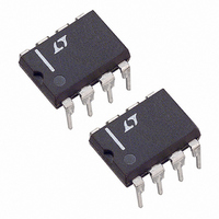
LTC1153CN8 Linear Technology, LTC1153CN8 Datasheet - Page 10

LTC1153CN8
Manufacturer Part Number
LTC1153CN8
Description
IC ELECTRNC CIRCUIT BREAKER 8DIP
Manufacturer
Linear Technology
Datasheet
1.LTC1153CS8PBF.pdf
(16 pages)
Specifications of LTC1153CN8
Applications
Overvoltage Protection, Circuit Breaker
Current - Supply
180µA
Voltage - Supply
4.5 V ~ 18 V
Operating Temperature
0°C ~ 70°C
Mounting Type
Through Hole
Package / Case
8-DIP (0.300", 7.62mm)
Lead Free Status / RoHS Status
Contains lead / RoHS non-compliant
Available stocks
Company
Part Number
Manufacturer
Quantity
Price
Company:
Part Number:
LTC1153CN8
Manufacturer:
LT
Quantity:
5 510
Company:
Part Number:
LTC1153CN8
Manufacturer:
MOT
Quantity:
5 510
Part Number:
LTC1153CN8
Manufacturer:
LT/凌特
Quantity:
20 000
LTC1153
A
The Y axis of the graph is normalized to one RC time
constant. The X axis is normalized to the set current. (The
set current is defined as the current required to develop
100mV across the drain sense resistor).
Note that the trip delay time is shorter for increasing levels
of MOSFET current. This ensures that the total energy
dissipated by the MOSFET is always within the bounds
established by the manufacturer for safe operation. (See
MOSFET data sheet for further S.O.A. information).
Using a Speed-Up Diode
Another way to reduce the trip delay time is to “bypass”
the delay resistor with a small signal diode as shown in
Figure 6. The diode will engage when the drop across the
drain sense resistor exceeds about 0.7V, providing a direct
path to the sense pin and dramatically reducing the trip
delay time. The drain sense resistor value is selected to
limit the maximum DC breaker current to 4A.
Reverse Battery Protection
The LTC1153 can be protected against reverse battery
conditions by connecting a resistor in series with the
ground lead as shown in Figure 7. The resistor limits the
supply current to less than 50mA with –12V applied. Since
the LTC1153 draws very little current while in normal
operation, the drop across the ground resistor is minimal.
the 5V P (or control logic) is protected by the 10k
resistors in series with the input and status pins.
10
PPLICATI
C
0.22 F
T
IN
C
STATUS
GND
T
Figure 6. Using a Speed-Up Diode
LTC1153
O
U
S
12V
DS
SD
V
G
S
I FOR ATIO
U
0.01 F
+
100 F
W
1N4148
1OOk
15V
LOAD
U
LTC1153 • F06
IRF530
0.036
Current Limited Power Supplies
The LTC1153 requires at least 3.5V at the supply pin to
ensure proper operation. It is therefore necessary that the
supply to the LTC1153 be held higher than 3.5V at all
times, even when the output of the switch is short circuited
to ground. The output voltage of a current limited regulator
may drop very quickly during short-circuit and pull the
supply pin of the LTC1153 below 3.5V before the shut-
down circuitry has had time to respond and remove drive
from the gate of the power MOSFET. A supply filter should
be added as shown in Figure 8 which holds the supply pin
of the LTC1153 high long enough for the over-current
shutdown circuitry to respond and fully discharge the
gate, i.e., break the circuit.
5V
CONTROL
>7V
LOGIC
P OR
5V
1 F
Figure 8. Supply Filter for Current Limited Supplies
+
IN
C
STATUS
GND
T
120k
100 F
Figure 7. Reverse Battery Protection
LTC1153
10k
10k
REGULATOR
+
5V/2A
C
0.47 F
300
T
10 F
DS
SD
V
G
S
IN
C
STATUS
GND
T
*SUPPLY FILTER COMPONENTS
*20
0.1 F
LTC1153
12V
+
+
*47 F
DS
SD
V
G
S
10 F
1N4148
10k
100k
15V
LOAD
MTP12N06
0.05
IRLR024
0.1
LTC1153 • F08
SHORT
CIRCUIT
LTC1153 • F07


