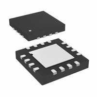
AT73C237 Atmel, AT73C237 Datasheet - Page 22

AT73C237
Manufacturer Part Number
AT73C237
Description
IC POWER MANAGEMENT UNIT 16QFN
Manufacturer
Atmel
Datasheet
1.AT73C237.pdf
(33 pages)
Specifications of AT73C237
Applications
Wireless
Current - Supply
250µA
Voltage - Supply
2.8 V ~ 5.5 V
Operating Temperature
-40°C ~ 85°C
Mounting Type
Surface Mount
Package / Case
16-QFN
Lead Free Status / RoHS Status
Lead free / RoHS Compliant
9.4
9.5
9.6
9.7
22
LDO4
High Performance Bandgap (HPBG)
Low Power Bandgap (LPBG)
Reset Generator
AT73C237
LDO4 is a 1.80V/2mA LDO with very low quiescent current. LDO4 can work with supply from
2.8V up to 5.5V. LDO4 requires a 1 µF output capacitor. It needs at least 300 mV of minimum
drop-out. LDO4 is always active once the pin VDD4 is supplied since it is used as internal refer-
ence supply. The VDD4 rail is independent from the other input rails (VDD1, 2, 3), allowing
LDO4 to be used to supply a Real Time Clock from a separate backup battery, for example.
Figure 9-4.
HPBG is a low power, low noise Band Gap circuit providing very accurate voltage reference to
LDOs that then can supply RF sections. HPBG operates in switching mode decreasing its cur-
rent consumption. Economic high performance Bandgap is particularly interesting when RF
LDOs are in idle mode (output voltage provided with very low output current e.g. <1mA). HPBG
is biased from an internal regulator supplied by VDD4, thus it is not active when only VDD3 is
present. HPBG requires at least external 100nF capacitor to achieve very low noise/high accu-
racy voltage reference.
HPBG is trimmed to 1.231V during product test.
LPBG is a low power Bandgap circuit used as reference voltage for LDO4. LPBG starts up as
soon as VDD4 is present and doesn't require any external capacitor for decoupling.
A Reset Generator produces an output reset (rising from “0” to “1”), called XRESO, at least 100
ms after the input reset state is activated. The input reset state can be produced by:
• VDD3 rising up, XRESIN not used or at “1”.
• External signal rising up on XRESIN and VDD3 present.
VDD
LDO4 Functional Diagram
AV
V
I
V
en3
BIAS
ESD
ZAP
BG
SS
V
BATC
V
ZAPC
GNDDC
GNDA
V
DD4
trcore <1:0>
sel4 <1:0>
vcore
vouts
V
IN
V
GNDA
6362A–PMAAC–01-Jul-08
O4
C
4


