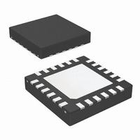
LM26480SQ-AA/NOPB National Semiconductor, LM26480SQ-AA/NOPB Datasheet - Page 28

LM26480SQ-AA/NOPB
Manufacturer Part Number
LM26480SQ-AA/NOPB
Description
IC REG BUCK/LDO DUAL 1.5A 24LLP
Manufacturer
National Semiconductor
Specifications of LM26480SQ-AA/NOPB
Applications
Processor
Voltage - Supply
2.8 V ~ 5.5 V
Operating Temperature
-40°C ~ 85°C
Mounting Type
Surface Mount
Package / Case
24-LLP
Operating Temperature (max)
85C
Operating Temperature (min)
-40C
Pin Count
24
Mounting
Surface Mount
Package Type
LLP EP
Case Length
4mm
Screening Level
Industrial
For Use With
LM26480SQ-AAEV - BOARD EVALUATION LM26480SQ-AA
Lead Free Status / RoHS Status
Lead free / RoHS Compliant
Current - Supply
-
Lead Free Status / Rohs Status
Compliant
Other names
LM26480SQ-AATR
Available stocks
Company
Part Number
Manufacturer
Quantity
Price
Company:
Part Number:
LM26480SQ-AA/NOPB
Manufacturer:
TI
Quantity:
3 400
Part Number:
LM26480SQ-AA/NOPB
Manufacturer:
NS/国半
Quantity:
20 000
www.national.com
High VIN-High Load Operation
Additional inforamtion is provided when the IC is operated at
extremes of VIN and regulator loads. These are described in
terms of the junction temperature and buck output ripple man-
agement.
Junction Temperature
The maximum junction temperature T
IC package.
The following equations demonstrate junction temperature
determination, ambient temperature T
power ust be controlled to keep T
T
Total IC power dissipation P
power dissipation of the four regulators plus a minor amount
for chip overhead. Chip overhead is bias, TSD and LDO ana-
log.
P
* VIN) [Watts].
J-MAX-OP
D-MAX
= PLOD1 + PLDO2 +PBUCK1 + PBUCK2 + (0.0001A
= T
A-MAX
+ (θ
JA
) [°C/Watt] * (P
D-MAX
J
is the sum of the individual
below this maximum:
J-MAX-OP
A-MAX
D-MAX
) [Watts]
of 125°C of the
and total chip
28
Power dissipation of LDO1 (PLDO1) = (VINLDO1 − VOUTL-
DO1) * IOUTLDO1 [V*A]
Power dissipation of LDO2 (PLDO2) = (VINLDO2 − VOUTL-
DO2) * IOUTLDO2 [V*A]
Power dissipation of Buck1 (PBuck1) = POUT − PIN = VOUT-
BUCK1 − IOUTBUCK1 * (1 − η2)/ η2 [V*A]
η1 = efficiency of Buck1
Power dissipation of Buck2 (PBuck2) = POUT − PIN = VOUT-
BUCK2 − IOUTBUCK2 * (1 − η2)/ η2 [V*A]
η2 = efficiency of Buck2
Where η is the efficiency for the specific condition is taken
from efficiency graphs.
If VIN and ILOADincrease, the output ripple associated with
the Buck Regulators also increases. This mainly occurs with
V
operation in this area of operation, it is recommended that the
system designer circumvents the output ripple issues by in-
stalling Schottky diodes on the bucks(s) that are expected to
perform under these extreme conditions.
IN
> 5.2V and a load current greater than 1.20A. To ensure


