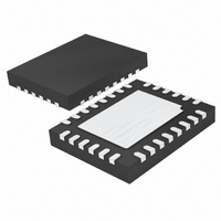
LTC3557EUF#PBF Linear Technology, LTC3557EUF#PBF Datasheet - Page 9

LTC3557EUF#PBF
Manufacturer Part Number
LTC3557EUF#PBF
Description
IC USB POWER MANAGE 28-QFN
Manufacturer
Linear Technology
Datasheet
1.LTC3557EUFPBF.pdf
(28 pages)
Specifications of LTC3557EUF#PBF
Applications
Handheld/Mobile Devices
Voltage - Supply
4.35 V ~ 5.5 V
Operating Temperature
-40°C ~ 85°C
Mounting Type
Surface Mount
Package / Case
28-QFN
Operating Temperature (max)
85C
Operating Temperature (min)
-40C
Pin Count
28
Mounting
Surface Mount
Package Type
QFN EP
Case Length
4mm
Screening Level
Industrial
Lead Free Status / RoHS Status
Lead free / RoHS Compliant
Current - Supply
-
Lead Free Status / Rohs Status
Compliant
Available stocks
Company
Part Number
Manufacturer
Quantity
Price
PIN FUNCTIONS
ILIM0, ILIM1 (Pins 1, 2): Input Current Control Pins. ILIM0
and ILIM1 control the input current limit. See Table 1. Both
pins are pulled low by a weak current sink.
WALL (Pin 3): Wall Adapter Present Input. Pulling this pin
above 4.3V will disconnect the power path from V
V
wall adapter has been detected.
LDO3V3 (Pin 4): Always On 3.3V LDO Output. The
LDO3V3 pin provides a regulated, always-on 3.3V supply
voltage. This pin gets its power from V
for light loads such as a real-time clock or housekeeping
microprocessor. A 1μF capacitor is required from LDO3V3
to ground if it will be called upon to deliver current. If
the LDO3V3 output is not used it should be disabled by
connecting it to V
SW1 (Pin 5): Power Transmission (Switch) Pin for
Step-Down Switching Regulator 1.
V
Regulator 1. This pin will generally be connected to V
FB1 (Pin 7): Feedback Input for Step-Down Switching
Regulator 1. This pin servos to a fi xed voltage of 0.8V when
the control loop is complete.
TYPICAL PERFORMANCE CHARACTERISTICS
OUT
IN1
0.85
0.84
0.83
0.82
0.81
0.80
0.79
0.78
0.77
0.76
0.75
. The ACPR pin will also be pulled low to indicate that a
0.1
(Pin 6): Power Input for Step-Down Switching
600mA Step-Down Switching
Regulator Feedback Voltage
vs Output Current
1
OUTPUT CURRENT (mA)
PULSE SKIP
OPERATION
Burst Mode
OUT
10
.
100
35571 G22
3.8V
5V
1000
OUT
. It may be used
0.85
0.84
0.83
0.82
0.81
0.80
0.79
0.78
0.77
0.76
0.75
0.1
400mA Step-Down Switching
Regulator Feedback Voltage
vs Output Current
BUS
OUT
1
OUTPUT CURRENT (mA)
PULSE SKIP
OPERATION
Burst Mode
.
to
10
MODE (Pin 8): Low Power Mode Enable. When this pin is
pulled high, the three step-down switching regulators are
set to low power Burst Mode operation.
EN1 (Pin 9): Logic Input Enables Step-Down Switching
Regulator 1.
EN2 (Pin 10): Logic Input Enables Step-Down Switching
Regulator 2.
EN3 (Pin 11): Logic Input Enables Step-Down Switching
Regulator 3.
FB3 (Pin 12): Feedback Input for Step-Down Switching
Regulator 3. This pin servos to a fi xed voltage of 0.8V when
the control loop is complete.
FB2 (Pin 13): Feedback Input for Step-Down Switching
Regulator 2. This pin servos to a fi xed voltage of 0.8V when
the control loop is complete.
RST2 (Pin 14): This is an open-drain output which indicates
that step-down switching regulator 2 has settled to its fi nal
value. It can be used as a power on reset for the primary
microprocessor or to enable the other buck regulators for
supply sequencing.
SW2 (Pin 15): Power Transmission (Switch) Pin for
Step-Down Switching Regulator 2.
100
35571 G23
3.8V
5V
T
A
1000
= 25°C unless otherwise specifi ed
LTC3557/LTC3557-1
50mV/DIV(AC)
200mA/DIV
1V/DIV
V
OUT1
V
I
OUT2
L1
0mA
EN1
0V
Step-Down Switching Regulator
Start-Up Waveform
V
I
MODE = 1
R
OUT2
OUT2
OUT1
= 50mA
= 1.2V
= 8Ω
100μs/DIV
35571fc
35571 G24
9


