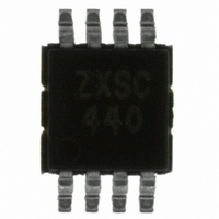
ZXSC440X8TA Diodes Zetex, ZXSC440X8TA Datasheet - Page 8

ZXSC440X8TA
Manufacturer Part Number
ZXSC440X8TA
Description
IC PHOTOFLASH CHARGER 8MSOP
Manufacturer
Diodes Zetex
Datasheet
1.ZXSC440X8TA.pdf
(16 pages)
Specifications of ZXSC440X8TA
Applications
Photoflash Capacitor Charger
Current - Supply
220µA
Voltage - Supply
1.8 V ~ 8 V
Operating Temperature
-40°C ~ 85°C
Mounting Type
Surface Mount
Package / Case
8-MSOP, Micro8™, 8-uMAX, 8-uSOP,
Lead Free Status / RoHS Status
Lead free / RoHS Compliant
Other names
ZXSC440X8TR
Output power calculation
This is approximately the power stored in the coil times
the frequency of operation times the efficiency.
Assuming a current of 1.2 amps in a 30µH primary, the
stored energy will be 21.6µJ. The frequency is set by
the time it takes the primary to reach 1.2 amps plus the
1.7µs time allowed to discharge the energy into the
reservoir capacitor. Using 3 volts, the ramp time is
12µs, so the frequency will be 73kHz, giving an input
power of about 1.6 watts. With an efficiency of 75% the
output power will be 1.2 watts. An 80µF capacitor
charged to 300 volts stores 3.6J, so 1.2 watts will take 3
seconds to charge it. Higher input voltages reduce the
ramp time, the frequency therefore goes up and the
output power is increased, resulting in shorter
charging times.
Output voltage adjustment
The ZXSC440 are adjustable output converters
allowing the end user the maximum flexibility. For
adjustable operation a potential divider network is
connected as follows:
ZXSC440
S E M I C O N D U C T O R S
8
The output voltage is determined by the equation:
In a circuit giving 300 volts, the "1" in the above
equation becomes negligible compared to the ratio
which is around 1000.
1000because of the negative input current in the
feedback pin. The resistor values, RA and RB, should
be maximized to improve efficiency and decrease
battery drain. Optimization can be achieved by
providing a minimum current of I
V
of the switching transistor, Q1.
In practice, there will be some stray capacitance across
RA and this will cause a lead in the feedback which can
affect hysteresis (it makes the device shut down too
early) and it is best to swamp this with a capacitor CA
and then use a capacitor CB across RB where CB/CA =
RA/RB.
compensating oscilloscope probes.
FB
pin. Output is adjustable from V
V
where V
OUT
This is similar to the method used for
= V
FB
FB
=300mV
(1 + RA / RB),
ISSUE 1 - JANUARY 2005
It will not be exactly
FB(MAX)
FB
to the (BR)V
=200nA to the
CEO


