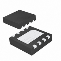
MAX8586ETA/V+T Maxim Integrated Products, MAX8586ETA/V+T Datasheet - Page 9

MAX8586ETA/V+T
Manufacturer Part Number
MAX8586ETA/V+T
Description
IC USB SWITCH 1.2A SGL 8-TDFN
Manufacturer
Maxim Integrated Products
Type
USB Switchr
Datasheet
1.MAX8586ETAT.pdf
(13 pages)
Specifications of MAX8586ETA/V+T
Number Of Outputs
1
Rds (on)
55 mOhm
Internal Switch(s)
Yes
Current Limit
1.2A
Voltage - Input
2.75 ~ 5.5 V
Operating Temperature
-40°C ~ 85°C
Mounting Type
Surface Mount
Package / Case
8-TDFN Exposed Pad
Lead Free Status / RoHS Status
Lead free / RoHS Compliant
When the MAX8586 die temperature exceeds +160°C,
the switch turns off and FAULT goes low. Thermal shut-
down does not utilize the 20ms fault-blanking timeout
period. When the junction temperature cools by 15°C,
the switch turns on again and FAULT returns high.
When an overload condition persists, the switch cycles
on and off, resulting in a pulsed output that reduces the
average system load.
A resistor from ISET to ground programs the current-
limit value. Use a resistor between 26kΩ and 60kΩ to
set the current limit according to the formula:
Do not use R
mum current rating of the device may be exceeded.
R
and do not provide a lower limit current than 500mA. If
the output drops below 1V (typ), the MAX8586 shifts to a
short-circuit current-limit threshold that is 30% above the
programmed level given by the I
To limit the input voltage drop during momentary output
load transients, connect a capacitor from IN to ground.
A 1µF ceramic capacitor is required for local decou-
pling; however, higher capacitor values further reduce
the voltage drop at the input. When driving inductive
loads, a larger capacitance may be needed to prevent
voltage spikes from exceeding the MAX8586’s absolute
maximum ratings.
A capacitor as large as 500µF is allowed on the output
to smooth out transients and/or increase rise/fall times.
Larger output capacitance may be used, but the result-
ing output charge time during startup may exceed the
fault-blanking period resulting in a FAULT flag.
A wide variety of devices (mice, keyboards, cameras,
and printers) typically connect to the USB port with
cables, adding an inductive component to the load. This
inductance causes the output voltage at the USB port to
oscillate during a load step. The MAX8586 drives induc-
tive loads; however, care must be taken to avoid
exceeding the device’s absolute maximum ratings.
Usually, the load inductance is relatively small, and the
MAX8586’s input includes a substantial bulk capaci-
tance from an upstream regulator as well as local
ISET
values larger than 60kΩ are not recommended
Input Power Supply and Capacitance
I
LIM(TYPICAL)
ISET
Applications Information
values below 26kΩ because the maxi-
_______________________________________________________________________________________
= 36400 / R
Setting the Current Limit
Driving Inductive Loads
Output Capacitance
Thermal Shutdown
LIM(TYPICAL)
ISET
(Amps)
formula.
Single 1.2A USB Switch in
bypass capacitors, limiting overshoot. If severe ringing
occurs because of large load inductance, clamp the
MAX8586 output below +6V and above -0.3V.
The MAX8586 features a slow turn-on and turn-off, mini-
mizing loading transients on the upstream power
source. SEL sets the active polarity of the logic inputs of
the MAX8586. Drive ON to the same logic state as SEL
to enable the output. Drive ON to the opposite logic
state as SEL to disable the output (see Table 1). The
output enters a high-impedance state when disabled.
Keep all input/output traces as short as possible to
reduce the effect of undesirable parasitic inductance
and optimize the switch response time to output short-
circuit conditions. Place input and output capacitors no
more than 5mm from device leads. Connect IN and OUT
to the power bus with short traces. Wide power bus
planes at IN and OUT provide superior heat dissipation
as well. An active switch dissipates little power with mini-
mal change in package temperature. Calculate the
power dissipation for this condition as follows:
At the normal operating current (I
maximum on-resistance of the switch (95mΩ), the
power dissipation is:
The worst-case power dissipation occurs when the out-
put current is just below the current-limit threshold with
an output voltage greater than 1V. In this case, the
power dissipated in the switch is the voltage drop
across the switch multiplied by the current limit:
For a 5.5V input and 1V output, the maximum power
dissipation is:
Table 1. SEL/ON Inputs
High
High
SEL
Low
Low
3mm x 3mm TDFN
P = 1.6A x (5.5V - 1V) = 7.2W
P = (0.5A)
Layout and Thermal Dissipation
Turn-On and Turn-Off Behavior
P = I
P = I
LIM
2
OUT
x (V
x 0.95Ω = 24mW
High
High
Low
Low
ON
2
IN
x R
- V
ON
OUT
OUT
)
= 0.5A) and the
OUT STATE
Disabled
Disabled
Enabled
Enabled
9


