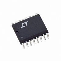
LTC1472CS#TR Linear Technology, LTC1472CS#TR Datasheet - Page 3

LTC1472CS#TR
Manufacturer Part Number
LTC1472CS#TR
Description
IC MATRIX SW PROT VCC/VPP 16SOIC
Manufacturer
Linear Technology
Type
PCMCIA/Cardbus Switchr
Datasheet
1.LTC1472CSPBF.pdf
(16 pages)
Specifications of LTC1472CS#TR
Number Of Outputs
1
Rds (on)
180 mOhm
Internal Switch(s)
Yes
Current Limit
1A
Voltage - Input
3.3V, 5V
Operating Temperature
0°C ~ 70°C
Mounting Type
Surface Mount
Package / Case
16-SOIC (3.9mm Width)
Lead Free Status / RoHS Status
Contains lead / RoHS non-compliant
Available stocks
Company
Part Number
Manufacturer
Quantity
Price
(VPP Switch Section) The
are at T
SYMBOL
V
VPP
V
I
I
I
I
R
VPP
VPP
I
V
V
I
I
t
t
t
t
t
t
t
t
Note 1: Absolute Maximum Ratings are those values beyond which the life
of the device may be impaired.
Note 2: V
programming enable inputs for desired output states.
Note 3: Power for the V
from the 5V
and 3.3V power is not required to control the NMOS V
Applications Information.)
Note 4: The two 3V
together and the two V
together. The 3V
and may drop to 0V when not required.
Note 5: The V
which reduces the short-circuit (0V) currents below peak permissible
current levels at higher output voltages.
ELECTRICAL CHARACTERISTICS
CCIN
PPIN
DD
VPPOUT
VPPEN
LIMVCC
LIMVPP
VPP1
VPP2
VPP3
VPP4
VPP5
VPP6
VPP7
VPP8
CC(IN)
DD
SDH
SDL
ON
IN
ENH
ENL
A
ENH
= 25°C. V
IN
PARAMETER
V
VPP Input Voltage Range
Logic Supply Voltage Range
V
VPP
V
Hi-Z Output Leakage Current
On Resistance VPP
On Resistance VPP
On Resistance VPP
VPP Enable Input High Voltage
VPP Enable Input Low Voltage
VPP Enable Input Current
SHDN Output High Voltage
SHDN Output Low Voltage
VPP
VPP
Delay and Rise Time
Delay and Rise Time
Delay and Rise Time
Delay and Fall Time
Delay and Fall Time
Delay and Fall Time
Output Turn-On Delay
Output Turn-On Delay
= 5V, V
CC
power supply which must be continuously powered. 12V
CC
CC(IN)
DD
IN
and VPP output are protected with foldback current limit
Input Voltage Range
IN
OUT
OUT
Supply Current, No Load
supply pins do not need to be continuously powered
IN
Supply Current, No Load
Supply Current, No Load
ENL
DD
Current Limit, V
Current Limit, VPP
supply input pins (14 and 15) must be connected
CC(OUT)
CC
= 0V. See V
= 5V, V
input logic and charge pump circuitry is derived
●
output pins (1 and 16) must be connected
OUT
OUT
OUT
denotes specifications which apply over the full operating temperature range, otherwise specifications
CC(IN)
CC
to VPP
to V
to GND
CC(IN)
and VPP Switch Truth Tables for
= 5V, VPP
IN
CC(IN)
IN
IN
CONDITIONS
(Note 7)
(Note 8)
Program to VPP
Program to 0V or Hi-Z
Program to VPP
Program to 0V or Hi-Z
Program to VPP
Program to V
Program to V
Program to 0V or Hi-Z
Program to Hi-Z, 0V < VPP
VPP
V
V
V
V
0V < VPP EN < VDD
Program to 0V, V
Program to VPP
Program to V
Program to VPP
From 0V to V
From 0V to VPP
From V
From VPP
From VPP
From V
From Hi-Z to V
From Hi-Z to VPP
= 12V, V
CC
CC(IN)
DD
DD
DD
switches. (See
IN
= 5V, I
= 5V
= 5V
= 12V, I
CC(IN)
CC(IN)
= 5V, I
IN
IN
CCEN0
SINK
to V
to 0V (Note 11)
CC(IN)
to VPP
to 0V, VPP
CC(IN)
CC(IN)
CC(IN)
LOAD
LOAD
CC(IN)
= 1mA
IN
IN
IN
IN
IN
CC(IN)
IN
CC(IN)
= V
IN
, I
, VPP
(Note 9)
or V
,VPP
, VPP
, VPP
, VPP
or V
= 5mA
= 120mA
SINK
(Note 9)
IN
(Note 9)
CCEN1
(Note 9)
(Note 10)
CC(IN)
CC(IN)
or Hi-Z, I
IN
OUT
IN
IN
IN
OUT
= 400µA
= 0V (Note 9)
= 0V (Note 11)
= 0V
= 12V
OUT
Note 6: To 90% of final value.
Note 7: 12V power is only required when VPP
The external 12V regulator can be shutdown at all other times. Built-in
charge pumps power the internal NMOS switches from the 5V V
when 12V is not present.
Note 8: Power for the VPP input logic and charge pump circuitry is derived
from the V
Note 9: To 90% of the final value, C
Note 10: To 10% of the final value, C
Note 11: To 50% of the initial value, C
= 0V (Note 5)
= 0V, (Note 2) unless otherwise noted.
= 0V (Note 5)
VPP
< 12V
LOAD
IN
= 12V
DD
= 400µA
power supply which must be continuously powered.
●
●
●
●
●
●
●
●
●
●
●
●
●
●
●
●
●
OUT
OUT
OUT
= 0.1µF, R
= 0.1µF, R
MIN
4.5
3.5
= 0.1µF, R
25
30
10
10
25
3
0
2
5
5
5
OUT
is programmed to 12V.
OUT
0.01
0.01
0.01
0.01
0.50
1.70
TYP
100
100
100
35
40
70
85
40
60
15
85
15
35
30
15
85
OUT
OUT
= 2.9k.
LTC1472
= 2.9k.
= 2.9k.
MAX
12.6
120
150
250
250
300
100
100
250
5.5
5.5
0.8
0.4
60
10
80
10
80
10
10
±1
50
50
50
1
5
DD
supply
UNITS
1472fa
3
mA
mA
µA
µA
µA
µA
µA
µA
µA
µA
µA
µA
µs
µs
µs
µs
µs
µs
µs
µs
Ω
Ω
Ω
V
V
V
V
V
V
V


