MC33981BPNA Freescale Semiconductor, MC33981BPNA Datasheet - Page 33
MC33981BPNA
Manufacturer Part Number
MC33981BPNA
Description
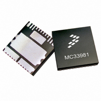
IC SWITCH HI SIDE SINGLE 16-PQFN
Manufacturer
Freescale Semiconductor
Type
High Side Switchr
Datasheet
1.MC33981BPNA.pdf
(37 pages)
Specifications of MC33981BPNA
Number Of Outputs
1
Rds (on)
4 mOhms
Internal Switch(s)
Yes
Current Limit
40A
Voltage - Input
6 ~ 27 V
Operating Temperature
-40°C ~ 125°C
Mounting Type
Surface Mount
Package / Case
16-PQFN, 16-PowerQFN
Lead Free Status / RoHS Status
Contains lead / RoHS non-compliant
Available stocks
Company
Part Number
Manufacturer
Quantity
Price

Part Number:
MC33981BPNA
Manufacturer:
FREESCALE
Quantity:
20 000


INTRODUCTION
datasheet. The addendum provides thermal performance information that may be
critical in the design and development of system applications. All electrical,
application, and packaging information is provided in the datasheet.
PACKAGING AND THERMAL CONSIDERATIONS
independently heating with P
T
temperature while only heat source 1 is heating with P
reference temperature while heat source 2 is heating with P
Rθ
This methodology is not meant to and will not predict the performance of a package in an application-specific environment. Stated
values were obtained by measurement and simulation according to the standards listed below.
STANDARDS
Table 7. Thermal Performance Comparison
Analog Integrated Circuit Device Data
Freescale Semiconductor
Notes
J1
Ρ
Ρ
Ρ
Ρ
This thermal addendum is provided as a supplement to the 33981 technical
This package is a dual die package. There are two heat sources in the package
For m, n = 1, Rθ
For m = 1, n = 2, Rθ
The stated values are solely for a thermal performance comparison of one package to another in a standardized environment.
J21
θJAmn
θJBmn
θJAmn
θJCmn
1.
2.
3.
4.
5.
and T
Resistance
Thermal
and Rθ
Per JEDEC JESD51-2 at natural convection, still air
condition.
2s2p thermal test board per JEDEC JESD51-7and
JESD51-5.
Per JEDEC JESD51-8, with the board temperature on the
center trace near the power outputs.
Single layer thermal test board per JEDEC JESD51-3 and
JESD51-5.
Thermal resistance between the die junction and the
exposed pad, “infinite” heat sink attached to exposed pad.
(1),
(2),
(1),
(5)
J2
(2)
(3)
(4)
, and a thermal resistance matrix with Rθ
J22,
T
T
J1
J2
ADDITIONAL DOCUMENTATION
respectively.
JA11
=
THERMAL ADDENDUM (REV 2.0)
1 = Power Chip, 2 = Logic Chip [°C/W]
m = 1,
n = 1
<1.0
JA12
is the thermal resistance from Junction 1 to the reference
7.0
22
62
R
R
θJA11
θJA21
is the thermal resistance from Junction 1 to the
1
and P
R
R
m = 1, n = 2
m = 2, n = 1
θJA12
θJA22
2
. This results in two junction temperatures,
4.0
0.0
18
48
.
P
P
1
2
m = 2,
n = 2
JAmn
1.0
41
27
81
1
.
.
2
. This applies to
Note: Recommended via diameter is 0.5 mm. PTH (plated through
hole) via must be plugged / filled with epoxy or solder mask in order
to minimize void formation and to avoid any solder wicking into the
via.
Figure 44. Surface mount for power PQFN
Note For package dimensions, refer to
the 33981 device datasheet.
with exposed pads
THERMAL ADDENDUM (REV 2.0)
ADDITIONAL DOCUMENTATION
12 MM X 12 MM
98ARL10521D
16-PIN PQFN
PNA SUFFIX
33981
16-PIN
PQFN
0.2 mm spacing
between PCB pads
0.2 mm spacing
between PCB pads
33981
33
Related parts for MC33981BPNA
Image
Part Number
Description
Manufacturer
Datasheet
Request
R


Part Number:
Description:
Manufacturer:
Freescale Semiconductor, Inc
Datasheet:
Part Number:
Description:
Manufacturer:
Freescale Semiconductor, Inc
Datasheet:
Part Number:
Description:
Manufacturer:
Freescale Semiconductor, Inc
Datasheet:
Part Number:
Description:
Manufacturer:
Freescale Semiconductor, Inc
Datasheet:
Part Number:
Description:
Manufacturer:
Freescale Semiconductor, Inc
Datasheet:
Part Number:
Description:
Manufacturer:
Freescale Semiconductor, Inc
Datasheet:
Part Number:
Description:
Manufacturer:
Freescale Semiconductor, Inc
Datasheet:
Part Number:
Description:
Manufacturer:
Freescale Semiconductor, Inc
Datasheet:
Part Number:
Description:
Manufacturer:
Freescale Semiconductor, Inc
Datasheet:
Part Number:
Description:
Manufacturer:
Freescale Semiconductor, Inc
Datasheet:
Part Number:
Description:
Manufacturer:
Freescale Semiconductor, Inc
Datasheet:
Part Number:
Description:
Manufacturer:
Freescale Semiconductor, Inc
Datasheet:
Part Number:
Description:
Manufacturer:
Freescale Semiconductor, Inc
Datasheet:
Part Number:
Description:
Manufacturer:
Freescale Semiconductor, Inc
Datasheet: