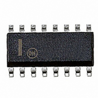
MC33368D ON Semiconductor, MC33368D Datasheet - Page 7

MC33368D
Manufacturer Part Number
MC33368D
Description
IC POWER FACTOR CTRLR HV 16-SOIC
Manufacturer
ON Semiconductor
Series
GreenLine™r
Datasheet
1.MC33368DR2G.pdf
(16 pages)
Specifications of MC33368D
Mode
Critical Conduction (CRM)
Current - Startup
16mA
Voltage - Supply
10 V ~ 16 V
Operating Temperature
-25°C ~ 125°C
Mounting Type
Surface Mount
Package / Case
16-SOIC (3.9mm Width)
Maximum Operating Temperature
+ 125 C
Mounting Style
SMD/SMT
Minimum Operating Temperature
- 25 C
Lead Free Status / RoHS Status
Contains lead / RoHS non-compliant
Frequency - Switching
-
Lead Free Status / Rohs Status
Lead free / RoHS Compliant
Available stocks
Company
Part Number
Manufacturer
Quantity
Price
Part Number:
MC33368D
Manufacturer:
ON/安森美
Quantity:
20 000
Company:
Part Number:
MC33368DG
Manufacturer:
ON Semiconductor
Quantity:
7
Part Number:
MC33368DR2
Manufacturer:
MOTOROLA/摩托罗拉
Quantity:
20 000
Company:
Part Number:
MC33368DR2G
Manufacturer:
ON
Quantity:
1 570
Part Number:
MC33368DR2G
Manufacturer:
MOTOROLA/摩托罗拉
Quantity:
20 000
INTRODUCTION
on line current harmonic content, there is an ever increasing
demand for an economical method of obtaining a unity
power factor. This data sheet describes a monolithic control
IC that was specifically designed for power factor control
with minimal external components. It offers the designer a
simple cost effective solution to obtain the benefits of active
power factor correction.
a bridge rectifier and a bulk storage capacitor to derive raw
dc voltage from the utility ac line, Figure 14.
when the instantaneous ac voltage exceeds the capacitor
voltage. This occurs near the line voltage peak and results in
a high charge current spike, Figure 15. Since power is only
taken near the line voltage peaks, the resulting spikes of
current are extremely nonsinusoidal with a high content of
harmonics. This results in a poor power factor condition
where the apparent input power is much higher than the real
power. Power factor ratios of 0.5 to 0.7 are common.
either a passive or active input circuit. Passive circuits
usually contain a combination of large capacitors, inductors,
and rectifiers that operate at the ac line frequency. Active
circuits incorporate some form of a high frequency
switching converter for the power processing with the boost
converter being the most popular topology. Since active
Rectified
Line
AC Line
AC Line
AC
Voltage
Current
Figure 15. Uncorrected Power Factor Input Waveforms
With the goal of exceeding the requirements of legislation
Most electronic ballasts and switching power supplies use
This simple rectifying circuit draws power from the line
Power factor correction can be achieved with the use of
V
DC
pk
0
0
Figure 14. Uncorrected Power Factor Circuit
Rectifiers
Line Sag
Bulk
Storage
Capacitor
Converter
FUNCTIONAL DESCRIPTION
http://onsemi.com
Load
7
input circuits operate at a frequency much higher than that
of the ac line, they are smaller, lighter in weight, and more
efficient than a passive circuit that yields similar results.
With proper control of the preconverter, almost any complex
load can be made to appear resistive to the ac line, thus
significantly reducing the harmonic current content.
Operating Description
protection features that are employed in modern high
performance current mode power supply controllers.
Referring to the block diagram in Figure 16, note that a
multiplier has been added to the current sense loop and that
this device does not contain an oscillator. A description of
each of the functional blocks is given below.
Error Amplifier
output is provided. The amplifier is a transconductance type,
meaning that it has high output impedance with controlled
voltage- -to- -current gain (g
input is internally biased at 5.0 V 2.0%. The output voltage
of the power factor converter is typically divided down and
monitored by the inverting input. The maximum input bias
current is - -1.0 mA which can cause an output voltage error
that is equal to the product of the input bias current and the
value of the upper divider resistor R2. The Error Amplifier
output is internally connected to the Multiplier and is pinned
out (Pin 4) for external loop compensation. Typically, the
bandwidth is set below 20 Hz so that the amplifier’s output
voltage is relatively constant over a given ac line cycle. In
effect, the error amplifier monitors the average output voltage
of the converter over several line cycles resulting in a fixed
Drive Output on- -time. The amplifier output stage can sink
and source 11.5 mA of current and is capable of swinging from
1.7 to 5.0 V, assuring that the Multiplier can be driven over its
entire dynamic range.
input is allowed to move independently with respect to the
output, since the compensation capacitor is connected to
ground. This allows dual usage of the Voltage Feedback pin
by the Error Amplifier and Overvoltage Comparator.
Overvoltage Comparator
the possibility of runaway output voltage. This condition
can occur during initial startup, sudden load removal, or
during output arcing and is the result of the low bandwidth
that must be used in the Error Amplifier control loop. The
Overvoltage Comparator monitors the peak output voltage
of the converter, and when exceeded, immediately
terminates MOSFET switching. The comparator threshold
is internally set to 1.08 V
during normal operation, the value of the output filter
capacitor C3 must be large enough to keep the peak- -to- -peak
ripple less than 16% of the average dc output.
The MC33368 contains many of the building blocks and
An Error Amplifier with access to the inverting input and
Note that by using a transconductance type amplifier, the
An Overvoltage Comparator is incorporated to eliminate
ref
m
. In order to prevent false tripping
¶ 50 mmhos). The noninverting


