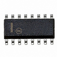
NCP1603D100R2 ON Semiconductor, NCP1603D100R2 Datasheet - Page 22

NCP1603D100R2
Manufacturer Part Number
NCP1603D100R2
Description
IC CTRLR PFC/PWM HV START 16SOIC
Manufacturer
ON Semiconductor
Datasheet
1.NCP1603D100R2.pdf
(30 pages)
Specifications of NCP1603D100R2
Mode
Critical Conduction (CRM), Discontinuous Conduction (DCM)
Frequency - Switching
58kHz
Current - Startup
17µA
Voltage - Supply
9 V ~ 18 V
Operating Temperature
-40°C ~ 125°C
Mounting Type
Surface Mount
Package / Case
16-SOIC (3.9mm Width)
Switching Frequency
405 KHz
Maximum Operating Temperature
+ 125 C
Mounting Style
SMD/SMT
Minimum Operating Temperature
- 40 C
Lead Free Status / RoHS Status
Contains lead / RoHS non-compliant
Other names
NCP1603D100R2OSTR
CRM in the same averaged input current. Hence, CRM is
generally preferred at around the sinusoidal peak for lower
the maximum current stress but DCM is also preferred at
the non−peak region to avoid excessive switching
frequencies. Because of the variable−frequency feature of
the CRM and constant−frequency feature of DCM,
switching frequency is the maximum in the DCM region
and hence the minimum switching frequency will be found
at the moment of the sinusoidal peak.
DCM PFC Circuit
Figure 58. Input voltage is a rectified 50 or 60 Hz
sinusoidal signal. The MOSFET is switching at a high
frequency (typically around 100 kHz) so that the inductor
current I
low−frequency components.
capacitor in order to eliminate the high−frequency content
of the DCM inductor current I
be too bulky because it can pollute the power factor by
distorting of the rectified sinusoidal input voltage.
PFC Methodology
particularly designed for both DCM and CRM operation.
The PFC methodology is described in this section.
switching cycle starts from zero in DCM. CRM is a special
DCM needs higher peak inductor current comparing to
A DCM/CRM PFC boost converter is shown in
Filter capacitor C
The PFC section uses a proprietary PFC methodology
As shown in Figure 59, the inductor current I
Inductor Current
Figure 58. DCM/CRM PFC Boost Converter
V
L
t
1
Figure 59. Inductor Current in DCM
in
I
in
basically consists of high−frequency and
filter
C
filter
I
L
t
2
T
is an essential and very small value
L
L
. This filter capacitor cannot
t
3
I
pk
L
of each
http://onsemi.com
C
bulk
V
time
out
22
case of DCM when t
MOSFET is on, the inductor current I
to I
voltage V
filter absorb the high−frequency component of inductor
current. It makes the input current I
signal.
formulated.
in Equations 6 and 7 are constant or slowly varying.
generated by a feedback signal V
modulation circuit and timing diagram are shown in
Figure 60. A relationship in Equation 8 is obtained.
the ramp capacitor C
Hence, according to Equation 8, the MOSFET on time t
is proportional to V
maximum voltage of V
V
ton(max)
The input filter capacitor C
From Equations 3, 4, and 5, the input impedance Z
Power factor is corrected when the input impedance Z
The MOSFET on time t
The charging current I
In order to protect the PFC modulation comparator, the
Ramp
pk
C
ramp
Figure 60. PFC Modulation Circuit and Timing
for a time duration t
12
in
(3.9 V typical) and the ramp pin (Pin 12) is with
. Equation 3 is formulated.
Z in +
ramp
out1
V
I in +
ton
Z in +
V in
I in
closed when
output low
I in +
ton
t 1 +
ramp
I pk (t 1 ) t 2 )
3
+
.
= 0. When the PFC boost converter
V in
I in
V in + L
Diagram
ch
2 T
I pk
ton
t 1 (t 1 ) t 2 )
is constant for a particular design.
2
C ramp V ton
+ 2L
I
ch
1
is constant 100 mA current and
1
2TL
is limited to internal clamp
filter
with inductance L and input
t 1
of PFC modulation duty is
for CRM
I ch
I pk
t 1
and the front−ended EMI
ton
for CRM
for DCM
and a ramp. The PFC
V
L
PWM
Comparator
for DCM
in
ton
increases from zero
+
−
a low−frequency
Turns off
MOSFET
(eq. 3)
(eq. 4)
(eq. 5)
(eq. 6)
(eq. 7)
(eq. 8)
in
is
in
1


