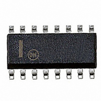
NCP1651DR2 ON Semiconductor, NCP1651DR2 Datasheet - Page 31

NCP1651DR2
Manufacturer Part Number
NCP1651DR2
Description
IC CTRLR PWR FACTOR SGL 16SOIC
Manufacturer
ON Semiconductor
Specifications of NCP1651DR2
Mode
Continuous Conduction (CCM), Discontinuous Conduction (DCM)
Frequency - Switching
250kHz
Current - Startup
8.5mA
Voltage - Supply
10 V ~ 18 V
Operating Temperature
-40°C ~ 125°C
Mounting Type
Surface Mount
Package / Case
16-SOIC (3.9mm Width)
Start-up Supply Current
5.5/8.5mA
Switching Freq
110kHz
Operating Supply Voltage (min)
-3V
Operating Supply Voltage (max)
18V
Operating Temp Range
-40C to 125C
Operating Temperature Classification
Automotive
Package Type
SOIC
Pin Count
16
Mounting
Surface Mount
Switching Frequency
110 KHz
Maximum Operating Temperature
+ 125 C
Mounting Style
SMD/SMT
Minimum Operating Temperature
- 40 C
Lead Free Status / RoHS Status
Contains lead / RoHS non-compliant
Other names
NCP1651DR2OS
Available stocks
Company
Part Number
Manufacturer
Quantity
Price
Part Number:
NCP1651DR2G
Manufacturer:
ON/安森美
Quantity:
20 000
needs a gain of - -25 dB at 10 Hz, since the forward gain is
equal to 25 dB at this frequency. The high frequency gain of
the error amplifier is:
A
connected from the output of the converter to the input of the
error amplifier. If the output circuit of Figure 42 is used, R
would be 9.31 k + 453 Ω, or 9.76 kΩ. A gain of - -25 dB is
equal to a divider ratio of:
A
so, R
or, R
The closest standard value resistor is 560 Ω.
amplifier should have a zero of 2 Hz or slightly higher. For
a 2 Hz zero, the compensation capacitor, C
calculated by:
be a good choice. This solution will provide a phase margin
of close to 90. In practice the value of capacitance could be
Vhf
V
--10
--15
For a crossover frequency of 10 Hz, the error amplifier
Where R
To offset the 2 Hz pole of the output filter, the error
100 mF is the closest standard value capacitor and would
40
35
30
25
20
15
10
--5
= 10
5
0
fb
fb
= R
0.01
= 0.056 x 9.76 kΩ = 546 Ω
/ R
(- -25/20)
fb
dc1
dc1
/ R
Figure 45. Forward Gain Plot
= 0.056
is the output voltage divider resistor that is
C fb =
0.1
dc1
= 0.056
2 π R fb 3 Hz
FREQUENCY (Hz)
1
1
= 95 mF
10
100
fb
can be
http://onsemi.com
1000
dc1
31
cut in half or more and probably remain stable. This can be
tested in the circuit, or simulated with a model in SPICE or
a similar analysis program.
in Figures 46 and 47. These include the effects of all of the
stages shown.
--105
--165
--180
--20
--40
--120
--135
--150
The gain and phase plots of the completed loop are shown
80
60
40
20
--75
--90
0
0.01
0.01
Figure 47. Loop Phase Plot
0.1
Figure 46. Loop Gain Plot
0.1
FREQUENCY (Hz)
FREQUENCY (Hz)
1
1
10
10
100
100
1000
1000


