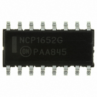
NCP1652DR2G ON Semiconductor, NCP1652DR2G Datasheet - Page 29

NCP1652DR2G
Manufacturer Part Number
NCP1652DR2G
Description
IC PFC CONTROLLER CCM/DCM 16SOIC
Manufacturer
ON Semiconductor
Datasheet
1.NCP1652DR2G.pdf
(34 pages)
Specifications of NCP1652DR2G
Mode
Continuous Conduction (CCM), Discontinuous Conduction (DCM)
Frequency - Switching
100kHz
Current - Startup
5.62mA
Voltage - Supply
9.3 V ~ 20 V
Operating Temperature
-40°C ~ 125°C
Mounting Type
Surface Mount
Package / Case
16-SOIC (3.9mm Width)
Switching Frequency
20 KHz to 250 KHz
Maximum Operating Temperature
+ 125 C
Mounting Style
SMD/SMT
Minimum Operating Temperature
- 40 C
Lead Free Status / RoHS Status
Lead free / RoHS Compliant
Other names
NCP1652DR2GOSTR
dependent of the average input current and the instantaneous
switch current. The gain of the average input current or slow
loop is given by Equation 9.
averaging circuit, the transconductance amplifier and the
gain of the AC error amplifier.
generated using a 4 kW resistor in the current sense amplifier
input. This proportional current is applied to a 21.33 kW at
the PWM comparator input to generate a current sense
voltage signal. The high frequency or fast loop gain, A
calculated using Equation 10.
the low frequency gain has to be less than one half of the high
frequency gain.
R
R
The control loop zero should be set at approximately at
1/10
capacitor is calculated using Equation 14.
Current Sense Resistor
controls the average input current and the second loop
controls the instantaneous current across the main switch.
The current sense signal affects both loops. The current
sense signal is fed into the positive input of the error
amplifier to control the average input current. In addition,
the current sense information together with the ramp
compensation and error amplifier signal control the
instantaneous primary peak current.
Equation 15,
AC_COMP
AC_COMP
The low frequency gain is the product of the current sense
A current proportional to the instantaneous current is
Equation 11 shows system stability requirements. That is,
Equation 12 is obtained by re-arranging Equation 11 for
The control loop zero, f
The PFC stage has two control loops. The first loop
The primary peak current, I
A
R
LF
th
IAVG
4k
of the oscillator frequency, f
+
. This equation provides the maximum value for
.
C
R
@ gm @ R
I
PK
f
IAVG
4k
AC_COMP
z
+
+
R
2p @ C
h @ V
AC_COMP
@ gm @ R
A
HF
AC_COMP
2 @ P
+
in(LL)
+
AC_COMP
Z
2p @
, is calculated using Equation 13.
out
21.33k
t
@ D
AC_COMP
4k
f
R
OSC
@ (2.286) t
1
10
)
IAVG
4666
PK
@ R
+ 5.333
0.88 @ 2 @ L
@ R
OSC
1
V
, is calculated using
@ gm
AC_COMP
in(LL)
AC_COMP
. The compensation
@ ( 2.286 )
@ t
5.333
on
2
P
(eq. 10)
(eq. 12)
(eq. 13)
(eq. 14)
(eq. 15)
(eq. 11)
(eq. 9)
http://onsemi.com
HF
, is
29
where, V
ratio, P
efficiency, L
time. Typical efficiency for this topology is around 88%.
signal resolution at the input of the ac reference amplifier.
The maximum voltage input of the ac reference amplifier to
prevent saturation is 4.5 V. This together with the
instantaneous peak current is used to calculate the current
sense resistor, R
Ramp Compensation
current-mode
conduction mode with a duty ratio greater than 50%.
Injecting a compensation ramp on the current sense signal
eliminates the subharmonic oscillations. The amount of
compensation is system dependent and it is determined by
the inductor falling di/dt.
system design. The amount of ramp compensation is set by
the user with a resistor, R
pin and ground. The Ramp Comp pin buffers the oscillator
ramp generated on the C
is internally mirrored with a 1:1.2 ratio. The inverted ac error
amplifier and the instantaneous switch current signals are
added to the ramp compensation mirrored current. The
resulting current signal is applied to an internal 21.33 kW
between the PWM Comparator non inverting input and
ground as shown in Figure 64.
compensation signal to the error signal, V
Equation 17.
where, V
typically 4.0 V.
match the falling di/dt (which has been converted to a dv/dt)
of the inductor at 50% duty cycle. Both the falling di/dt and
output voltage need to be reflected by the transformer turns
ratio to the primary side. Equations 18 through 23 assist in
the derivation of equations for R
V
The current sense resistor is selected to achieve maximum
Subharmonic oscillations are observed in peak
The NCP1652 has built in ramp compensation to facilitate
The maximum voltage contribution of the ramp
For proper ramp compensation, the ramp signal should
RCOMP
out
dt
in(LL)
primary
CT(peak)
is the output power, P
+
di
dt
P
( 1.2 ) @ V
secondary
is the low line ac input voltage, D is the duty
is the primary inductance and t
R
CS
di
+
controllers
CS
, using Equation 16.
is the oscillator ramp peak voltage,
dt
+ 4.5
secondary
+
CT(peak)
R
di
T
RCOMP
RCOMP
V
L
pin. The current across R
4k @ V
R
out
S
IAVG
@
+
operating
in
@ ( 21.33k )
N
N
, between the Ramp Comp
CS
V
@ P
S
P
is the input power, h is the
in(LL)
L
out
P
+
and R
in
@
V
@ 2
@ D
L
out
P
RCOMP
N
N
COMP
+
N
N
P
S
in
P
S
R
102.38k
2
RCOMP
on
.
, is given by
continuous
is the on
(eq. 16)
(eq. 17)
(eq. 18)
(eq. 19)
RCOMP


