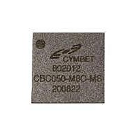
CBC050-M8C Cymbet Corporation, CBC050-M8C Datasheet - Page 4

CBC050-M8C
Manufacturer Part Number
CBC050-M8C
Description
IC BATT SOLID ST ENERCHIP 16QFN
Manufacturer
Cymbet Corporation
Series
EnerChip™r
Type
Thin Filmr
Datasheet
1.CBC050-M8C-TR1.pdf
(4 pages)
Specifications of CBC050-M8C
Capacity
50µAh
Voltage - Output
3.8V
Operating Temperature
-20°C ~ 70°C
Package / Case
16-QFN
Battery Size
8 mm x 8 mm
Length
8 mm
Rechargeable/non-rechargeable
Rechargeable
Width
8 mm
Output Voltage
3.8 V
Termination Style
Solder
Lead Free Status / RoHS Status
Lead free / RoHS Compliant
For Use With
859-1002 - ENERCHIP EH SEH EVAL KIT859-1000-5 - ENERCHIP EH CBC5300 MODULE
Lead Free Status / Rohs Status
Lead free / RoHS Compliant
Other names
859-1005-5
Available stocks
Company
Part Number
Manufacturer
Quantity
Price
Company:
Part Number:
CBC050-M8C
Manufacturer:
CYMBET
Quantity:
210
Part Number:
CBC050-M8C
Manufacturer:
CYMBET
Quantity:
20 000
Printed Circuit Board (PCB) Layout Guidelines and Recommendations
Electrical resistance of solder flux residue on PCBs can be low enough to partially or fully discharge the backup
energy cell and in some cases can be comparable to the load typically imposed on the cell when delivering
power to an integrated circuit in low power mode. Therefore, solder flux must be thoroughly washed from the
board following soldering. The PCB layout can make this problem worse if the cell’s positive and negative
terminals are routed near each other and under the package, where it is difficult to wash the flux residue away.
To avoid this situation, make sure positive and negative traces are routed outside of the package footprint to
ensure that flux residue will not cause a discharge path between the positive and negative pads. Similarly, a
leakage current path can exist from the package lead solder pads to the exposed die pad on the underside of
the package as well as any solder pad on the PCB that would be connected to that exposed die pad during the
reflow solder process. Therefore, it is strongly recommended that the PCB layout not include a solder pad in the
region where the exposed die pad of the package will land. It is sufficient to place PCB solder pads only where
the package leads will be. That region of the PCB where the exposed die pad will land must not have any solder
pads, traces, or vias.
When placing a silk screen on the PCB around the perimeter of the package, place the silk screen outside of
the package and all metal pads. Failure to observe this precaution can result in package cracking during solder
reflow due to the silk screen material interfering with the solder solidification process during cooling.
A recommended CBC050 PCB layout is shown in Figure 1 below. Notice that there should not be a center pad
on the PCB to mate with the exposed die pad on the CBC050 package. Again, this is to reduce the possible
number and severity of leakage paths between the EnerChip terminals.
Soldering, Rework, and Electrical Test
Refer to the Cymbet User Manual for soldering, rework, and replacement of the EnerChip on printed circuit
boards, and for instructions on in-circuit electrical testing of the EnerChip.
Disclaimer of Warranties; As Is
The information provided in this data sheet is provided “As Is” and Cymbet Corporation disclaims all representations or warranties of any
kind, express or implied, relating to this data sheet and the Cymbet EnerChip product described herein, including without limitation, the
implied warranties of merchantability, fitness for a particular purpose, non-infringement, title, or any warranties arising out of course of
dealing, course of performance, or usage of trade. Cymbet EnerChip products are not approved for use in life critical applications. Users
shall confirm suitability of the Cymbet EnerChip product in any products or applications in which the Cymbet EnerChip product is adopted
for use and are solely responsible for all legal, regulatory, and safety-related requirements concerning their products and applications and
any use of the Cymbet EnerChip product described herein in any such product or applications.
DS-72-01 Rev B
Figure 1: Recommended PCB layout for the CBC050 package. Do not route signal traces under the EnerChip
as they could become shorted to the die pad (as shown by the dotted lines) on the package underside.
Cymbet, the Cymbet Logo and EnerChip are trademarks of Cymbet Corporation. All Rights Reserved
©2009-2010 Cymbet Corporation • Tel: +1-763-633-1780 • www.cymbet.com
EnerChip™ CBC050 Solid State Energy Storage
3
2
1
4
16
5
15
6
14
7
13
8
11
10
12
9
Dimensions in inches [mm]
Page 4 of 4


