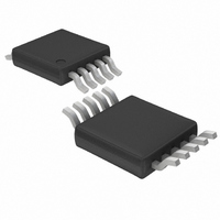
LT4351IMS Linear Technology, LT4351IMS Datasheet - Page 12

LT4351IMS
Manufacturer Part Number
LT4351IMS
Description
IC CTRLR MOSFET DIODE-OR 10MSOP
Manufacturer
Linear Technology
Datasheet
1.LT4351IMSPBF.pdf
(20 pages)
Specifications of LT4351IMS
Applications
Paralleled/Redundant Power Supplies
Fet Type
N-Channel
Number Of Outputs
1
Internal Switch(s)
No
Delay Time - Off
600ns
Voltage - Supply
1.2 V ~ 18 V
Current - Supply
1.4mA
Operating Temperature
-40°C ~ 85°C
Mounting Type
Surface Mount
Package / Case
10-MSOP, Micro10™, 10-uMAX, 10-uSOP
Lead Free Status / RoHS Status
Contains lead / RoHS non-compliant
Delay Time - On
-
Available stocks
Company
Part Number
Manufacturer
Quantity
Price
Part Number:
LT4351IMS
Manufacturer:
LT/凌特
Quantity:
20 000
Part Number:
LT4351IMS#PBF
Manufacturer:
LINEAR/凌特
Quantity:
20 000
LT4351
As an example, for 500nH of inductance and R
100mΩ, then:
Check vendor data for ESR and iterate to get the best
value. Additional C
concerns.
If the boost regulator is being used, place a 10µF low ESR
ceramic capacitor from V
0.1µF ceramic capacitor close to V
capacitors should have low ESR (less than 10mΩ for the
10µF and 40mΩ for the 0.1µF). These capacitors help to
eliminate problems associated with noise produced by the
boost regulator. They are decoupled from the V
by a small 1Ω resistor, as shown in Figure 8. The LT4351
will perform better with a small ceramic capacitor (10µF)
on OUT to GND.
External Boost Supply
The V
this case, simply omit the boost regulator inductor and
diode and leave the SW pin open. Suitable V
(minimum of a 1µF ceramic) should remain due to the
current pulses required for the gate driver.
The V
current required to charge the MOSFET’s gate which is
dependent on the gate charge required and frequency of
switching. Typically the average current will be under 10mA.
APPLICATIONS INFORMATION
12
C ≥
DD
DD
4 • 500nF
current consists of 3.5mA of DC current with the
pin may be powered by an external supply. In
0.1
2
= 200µF
B
capacitance may be required for load
IN
to GND. Place a 10µF and a
V
IN
PARASITIC
IN
L
IN
and GND. These
DD
ESR
capacitance
C
IN
B
Figure 8. V
of about
supply
C
10µF
V3
1Ω
IN
C
10µF
V1
Capacitors
MOSFET Selection
The LT4351 uses either a single N-channel MOSFET or
back-to-back N-channel MOSFETs as the pass element.
Back-to-back MOSFETs prevent the MOSFET body diode
from passing current.
Use a single MOSFET if current flow is allowable from
input to output when the input supply is above the output
(limited overvoltage protection). In this case the MOSFET
should have a source on the input side so the body diode
conducts current to the load. Back-to-back MOSFETs are
normally connected with their sources tied together to
provide added protection against exceeding maximum
gate to source voltage.
Selection of MOSFETs should be based on R
and BV
breakdown when V
R
power rating at the maximum load current (I
BV
GATE to 7.5V above the lesser of V
to-back MOSFETs where sources are tied together, this
allows the use of MOSFETs with a VGS max rating of 8V
or more. If a single MOSFET is used, care must be taken
to ensure the VGS max rating is not exceeded. When the
MOSFET is turned off, the GATE voltage is near ground,
the source at V
than V
If a single MOSFET is used with source to V
should be greater than the maximum V
gate is at 0.2V when off.
DS(ON)
GSS
C
0.1µF
V2
IN(MAX)
should be at least 8V. The LT4351 will clamp the
GSS
should be selected to keep within the MOSFET
V
GND
. BV
IN
LT4351
GATE
.
IN
4351 F08
DSS
. Thus, MOSFET VGS max must be greater
IN
should be high enough to prevent
or OUT are at their maximum value.
IN
IN
or OUT. For back-
since the MOSFET
IN
DS(ON)
, then BV
2
• R
, BV
DS(ON)
4351fc
DSS
GSS
)


