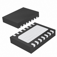
LTC4358CDE#TRPBF Linear Technology, LTC4358CDE#TRPBF Datasheet

LTC4358CDE#TRPBF
Specifications of LTC4358CDE#TRPBF
Available stocks
Related parts for LTC4358CDE#TRPBF
LTC4358CDE#TRPBF Summary of contents
Page 1
... If the power source fails or is shorted, a fast turnoff minimizes reverse current transients. L, LT, LTC and LTM are registered trademarks of Linear Technology Corporation. All other trademarks are the property of their respective owners. Power Dissipation vs Load Current 3 ...
Page 2
... JMAX JC ORDER INFORMATION LEAD FREE FINISH TAPE AND REEL LTC4358CDE#PBF LTC4358CDE#TRPBF LTC4358IDE#PBF LTC4358IDE#TRPBF LTC4358CFE#PBF LTC4358CFE#TRPBF LTC4358IFE#PBF LTC4358IFE#TRPBF Consult LTC Marketing for parts specifi ed with wider operating temperature ranges. *Temperature grades are identifi label on the shipping container. ...
Page 3
ELECTRICAL CHARACTERISTICS temperature range, otherwise specifi cations are at T SYMBOL PARAMETER V Operating Supply Range DD I Operating Supply Current Pin Current IN I OUT Pin Current OUT I DRAIN Pin Current DRAIN ΔV N-Channel Gate ...
Page 4
LTC4358 TYPICAL PERFORMANCE CHARACTERISTICS V Current ( 500 OUT DD 400 300 200 100 (V) DD 4358 G01 MOSFET R vs Temperature DS(ON) ...
Page 5
PIN FUNCTIONS (DE/FE PACKAGES) DRAIN: The exposed pad is the drain of the internal N-channel MOSFET. This pin must be connected to OUT (Pin 9/Pin 10). GATE: Gate Drive Output. If reverse current fl ows, a fast pulldown circuit quickly ...
Page 6
LTC4358 OPERATION High availability systems often employ parallel-connected power supplies or battery feeds to achieve redundancy and enhance system reliability. ORing diodes have been a popular means of connecting these supplies at the point of load. The disadvantage of this ...
Page 7
APPLICATIONS INFORMATION ORing Two Supply Outputs Where LTC4358s are used to combine the outputs of two supplies, the power supply with the highest output voltage sources most or all of the current. If this supply’s output is quickly shorted to ...
Page 8
LTC4358 APPLICATIONS INFORMATION V Hold-Up Circuit DD In the event of an input short, parasitic inductance between the input supply of the LTC4358 and the load bypass capacitor may cause V to glitch below its minimum DD operating voltage. This ...
Page 9
APPLICATIONS INFORMATION GND Figure 4. DFN Layout Considerations for 1” OUT × 1” Single Sided PCB 0.1 3.5 4.0 5.0 6.0 3.0 4.5 5.5 ...
Page 10
LTC4358 PACKAGE DESCRIPTION 3.60 ±0.05 2.20 ±0.05 1.70 ± 0.05 RECOMMENDED SOLDER PAD PITCH AND DIMENSIONS APPLY SOLDER MASK TO AREAS THAT ARE NOT SOLDERED PIN 1 TOP MARK (SEE NOTE 6) 0.200 REF NOTE: 1. DRAWING PROPOSED TO BE ...
Page 11
... DIMENSIONS ARE IN 3. DRAWING NOT TO SCALE Information furnished by Linear Technology Corporation is believed to be accurate and reliable. However, no responsibility is assumed for its use. Linear Technology Corporation makes no representa- tion that the interconnection of its circuits as described herein will not infringe on existing patent rights. FE Package 16-Lead Plastic TSSOP (4 ...
Page 12
... Monitor LTC4357 Positive High Voltage Ideal Diode Controller LTC4223-1/LTC4223-2 Dual Supply Hot Swap Controller for Advanced Mezzanine Cards and μTCA Hot Swap is a trademark of Linear Technology Corporation. 12 Linear Technology Corporation 1630 McCarthy Blvd., Milpitas, CA 95035-7417 (408) 432-1900 FAX: (408) 434-0507 ● ...


