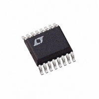
LTC1473LCGN Linear Technology, LTC1473LCGN Datasheet - Page 9

LTC1473LCGN
Manufacturer Part Number
LTC1473LCGN
Description
IC SWITCH DVR PWRPATH DUAL16SSOP
Manufacturer
Linear Technology
Series
PowerPath™r
Datasheet
1.LTC1473LCGNPBF.pdf
(16 pages)
Specifications of LTC1473LCGN
Applications
Handheld/Mobile Devices
Fet Type
N-Channel
Number Of Outputs
2
Internal Switch(s)
No
Delay Time - On
22µs
Delay Time - Off
1µs
Voltage - Supply
2.8 V ~ 9 V
Current - Supply
100µA
Operating Temperature
0°C ~ 70°C
Mounting Type
Surface Mount
Package / Case
16-SSOP
Power Switch Family
LTC1473L
Mounting
Surface Mount
Supply Current
100uA
Package Type
SSOP N
Operating Temperature (min)
0C
Operating Temperature (max)
70C
Operating Temperature Classification
Commercial
Pin Count
16
Lead Free Status / RoHS Status
Contains lead / RoHS non-compliant
Available stocks
Company
Part Number
Manufacturer
Quantity
Price
Company:
Part Number:
LTC1473LCGN
Manufacturer:
LT
Quantity:
10 000
Part Number:
LTC1473LCGN
Manufacturer:
LINEAR/凌特
Quantity:
20 000
Company:
Part Number:
LTC1473LCGN#PBF
Manufacturer:
Linear Technology
Quantity:
135
Part Number:
LTC1473LCGN#PBF
Manufacturer:
LINEAR/凌特
Quantity:
20 000
APPLICATIO S I FOR ATIO
The back-to-back topology also allows for independent
control of each half of the switch pair which facilitates
bidirectional inrush current limiting and the so-called
“2-diode mode” described in the following section.
The 2-Diode Mode
Under normal operating conditions, both halves of each
switch pair are turned on and off simultaneously. For
example, when the input power source is switched from
BAT1 to DCIN in Figure 4, both gates of switch pair SW
A1/B1 are normally turned off and both gates of switch pair
SW A2/B2 are turned on. The back-to-back body diodes in
switch pair, SW A1/B1, block current flow in or out of the
BAT1 input connector.
In the “2-diode mode,” only the first half of each power
path switch pair, i.e., SW A1 and SW A2, is turned on; and
the second half, i.e., SW B1 and SW B2, is turned off. These
two switch pairs now act simply as two diodes connected
to the two main input power sources as illustrated in
Figure 4. The power path diode with the highest input
voltage passes current through to the output load to
ensure that the output is powered even under start-up or
abnormal operating conditions. (An undervoltage lockout
circuit defeats this mode when the V
2.5V. The supply to V
U
BAT1
DCIN
+
U
comes from the main power
ON
SW A1
Figure 4. LTC1473L PowerPath Switches in 2-Diode Mode
W
+
pin drops below
SW B1
OFF
U
ON
SW A2
LTC1473L
SW B2
sources, DCIN and BAT1 through two common cathode
Schottky diodes as shown in Figure 1.)
The 2-diode mode is asserted by applying an active low to
the DIODE input.
COMPONENT SELECTION
N-Channel Switches
The LTC1473L adaptive inrush limiting circuitry permits
the use of a wide range of logic-level N-Channel MOSFET
switches. A number of dual low R
in 8-lead surface mount packages are available that are
well suited for LTC1473L applications.
The maximum allowable drain-source voltage, V
of the two switch pairs, SW A1/B1 and SW A2/B2 must be
high enough to withstand the maximum input DC supply
voltage. Since the DC supply is in the 3.3V to 10V range,
12V MOSFET switches will suffice.
As a general rule, select the switch with the lowest
R
mize the heat dissipated in the switches while increasing
the overall system efficiency. Higher switch resistances
can be tolerated in some systems with lower current
requirements, but care should be taken to ensure that the
OFF
DS(ON)
at the maximum allowable V
R
SENSE
1473 F04
+
C
IN
OUTPUT
LOAD
DS(ON)
LTC1473L
N-channel switches
DS
. This will mini-
DS(MAX)
9
,


