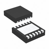
LTC4352IDD#PBF Linear Technology, LTC4352IDD#PBF Datasheet - Page 11

LTC4352IDD#PBF
Manufacturer Part Number
LTC4352IDD#PBF
Description
IC IDEAL DIODE CNTRL 12-DFN
Manufacturer
Linear Technology
Datasheet
1.LTC4352CMSPBF.pdf
(16 pages)
Specifications of LTC4352IDD#PBF
Applications
Redundant Power Supplies, Telecom Infrastructure
Fet Type
N-Channel
Number Of Outputs
1
Internal Switch(s)
No
Delay Time - On
250ns
Delay Time - Off
200ns
Voltage - Supply
2.9 V ~ 18 V
Current - Supply
1.4mA
Operating Temperature
-40°C ~ 85°C
Mounting Type
Surface Mount
Package / Case
12-DFN
Lead Free Status / RoHS Status
Lead free / RoHS Compliant
Available stocks
Company
Part Number
Manufacturer
Quantity
Price
External CPO Supply
The internal charge pump takes milliseconds to charge
up the CPO pin capacitor especially during device power
up. This time can be shortened by connecting an external
supply to the CPO pin. A series resistor is needed to limit
the current into the internal clamp between the CPO and
SOURCE pins. The CPO supply should also be higher than
the main input supply to meet the gate drive requirements
of the MOSFET. Figure 7 shows such a 5V ideal diode ap-
plication, where a 12V supply is connected to the CPO pin
through a 1k resistor. The 1k limits the current into the
CPO pin to 5.3mA, when the SOURCE pin is grounded.
Input Transient Protection
When the capacitances at the input and output are very
small, rapid changes in current can cause transients that
exceed the 24V Absolute Maximum Rating of the V
OUT pins. In ORing applications using a single MOSFET, one
surge suppressor connected from OUT to ground clamps
all the inputs. In the absence of a surge suppressor, an
output capacitance of 10μF is sufficient in most applications
to prevent the transient from exceeding 24V. Back-to-back
MOSFET applications, depending on voltage levels, may
require a surge suppressor on each supply input.
applicaTions inForMaTion
Figure 7. 5V Ideal Diode with External 12V Powering CPO for
Faster Start-up and Refresh
R7
1k
12V
5V
0.1µF
C2
IN
and
SOURCE
CPO
V
IN
Si7336ADP
LTC4352
GATE
GND
Design Example
The following design example demonstrates the calcula-
tions involved for selecting components in a 12V system
with 10A maximum load current (see Figure 1).
First, calculate the R
desired forward drop at full load. Assuming a V
50mV (which is comfortably below the 200mV minimum
open MOSFET fault threshold):
The Si7336ADP offers a good solution, in a SO-8 sized
package, with a maximum R
30V. The maximum power dissipation in the MOSFET is:
With a maximum steady-state thermal resistance, θ
of 65°C/W, 0.4W causes a modest 26°C rise in junction
temperature of the Si7336ADP above the ambient.
The input capacitance, C
6500pF . Slightly exceeding the 10x recommendation, a
0.1µF capacitor is selected for C2.
Q1
P = I
R
DS ON
OUT
4352 F07
( ) ≤
2
LOAD
TO LOAD
I
V
• R
LOAD
FWD
DS(ON)
=
DS(ON)
50mV
10A
= (10A)
ISS
of the MOSFET to achieve the
, of the Si7336ADP is about
= 5mΩ
DS(ON)
2
• 4mΩ = 0.4W
of 4mΩ and BV
LTC4352
11
FWD
DSS
4352fa
JA
of
of
,


