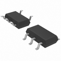
LTC4411ES5#TRMPBF Linear Technology, LTC4411ES5#TRMPBF Datasheet - Page 5

LTC4411ES5#TRMPBF
Manufacturer Part Number
LTC4411ES5#TRMPBF
Description
IC IDEAL DIODE LOW LOSS TSOT23-5
Manufacturer
Linear Technology
Datasheet
1.LTC4411ES5TRMPBF.pdf
(8 pages)
Specifications of LTC4411ES5#TRMPBF
Applications
Handheld/Mobile Devices
Fet Type
P-Channel
Number Of Outputs
1
Internal Switch(s)
Yes
Delay Time - On
1.2µs
Delay Time - Off
1.1µs
Voltage - Supply
2.6 V ~ 5.5 V
Current - Supply
40µA
Operating Temperature
-40°C ~ 85°C
Mounting Type
Surface Mount
Package / Case
TSOT-23-5, TSOT-5, TSOP-5
Lead Free Status / RoHS Status
Lead free / RoHS Compliant
Other names
LTC4411ES5#PBF
LTC4411ES5#PBF
LTC4411ES5#TRMPBF
LTC4411ES5#TRMPBFTR
LTC4411ES5#PBF
LTC4411ES5#TRMPBF
LTC4411ES5#TRMPBFTR
Available stocks
Company
Part Number
Manufacturer
Quantity
Price
BLOCK DIAGRA
OPERATIO
The LTC4411 operation is described with the aid of
Figure 3. Forward regulation for the LTC4411 has three
operation modes depending on the magnitude of the load
current. For small load currents, the LTC4411 will provide
a constant voltage drop; this operating mode is referred to
as “constant V
the voltage drop will increase linearly with the current with
a slope of 1/R
“constant R
ther, exceeding I
crease rapidly; this operating mode is referred to as
“constant I
following parameters: R
are specified with the aid of Figure 3.
Operation begins when the power source at IN rises above
the UVLO voltage of 2.4V (typ) and the CTL (control) pin
is low. If only the voltage at the IN pin is present, the power
source to LTC4411 (V
The amplifier (A) will deliver a voltage proportional to the
difference between V
internal P-channel MOSFET (P1), driving this gate voltage
below V
be pulled up towards V
V
is now in forward regulation and the load at OUT will be
GATE
to maintain a low forward voltage drop. The system
IN
. This will turn on P1. As P1 conducts, V
ON
ON
GND
CTL
IN
ON
” regulation. The characteristics for the
” regulation. As the current increases fur-
ON
1
2
3
” regulation. As the current exceeds I
; this operating mode is referred to as
MAX
U
3µA
V
REF
IN
, the forward voltage drop will in-
DD
and V
IN
) will be supplied from the IN pin.
FWD
. The LTC4411 will then control
W
V
B
, R
OUT
ON
to the gate (V
, V
FWD
, I
Figure 2. Detailed Block Diagram
FWD
GATE
+
OFF
–
, and I
–
OUT
) of the
+
+
–
FWD
MAX
will
powered from the supply at IN. As the load current varies,
V
drop. If the load current exceeds P1’s ability to deliver the
current, as V
a fixed resistor, with resistance R
voltage will increase with increased load current. As I
increases further (I
the load current as described below. During the forward
regulation mode of operation the STAT pin will be an open
circuit.
+
GATE
A
P1
V
GATE
–
will be controlled to maintain a low forward voltage
I
I
MAX
FWD
I
OC
SHDB
3.0
2.5
2.0
1.5
1.0
0.5
GATE
0
Figure 3. LTC4411 vs Schottky Diode
Forward Conduction Characteristics
V
0
FWD
T
A
LTC4411
= 40°C
OUT
approaches GND, the P1 will behave as
UVLO
LOAD
MAX
0.25
SLOPE
1/R
FORWARD VOLTAGE (V)
FWD
> I
OVERTEMP
SLOPE
1/R
MAX
ON
0.5
SCHOTTKY
DIODE
), the LTC4411 will regulate
V
B
ON
, whereby the forward
0.75
10µA
LTC4411
4411 F03
5
4
4411 F02
1.0
OUT
STAT
LOAD
4411fa
5


