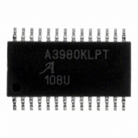
A3980KLP-T Allegro Microsystems Inc, A3980KLP-T Datasheet - Page 11

A3980KLP-T
Manufacturer Part Number
A3980KLP-T
Description
IC MOTOR DRIVER MICROSTEP 28-TSS
Manufacturer
Allegro Microsystems Inc
Datasheet
1.A3980KLPTR-T.pdf
(18 pages)
Specifications of A3980KLP-T
Applications
Stepper Motor Driver
Number Of Outputs
1
Current - Output
± 1A
Voltage - Load
7 V ~ 50 V
Voltage - Supply
3 V ~ 5.5 V
Operating Temperature
-40°C ~ 125°C
Mounting Type
Surface Mount
Package / Case
28-TSSOP Exposed Pad, 28-eTSSOP, 28-HTSSOP
Lead Free Status / RoHS Status
Lead free / RoHS Compliant
Other names
620-1081
A3980
as shown in table 3. In all other modes, V
allowed to exceed 4 V, because the peak sense value can
reach V
Fixed Off-Time.
circuitry uses a one-shot circuit to control the duration of
time that the DMOS FETs remain off. The one shot off-time,
t
nation of an external resistor (R
combination is connected from the timing terminal RC1 to
ground, and the other similarly connected to RC2 . t
is approximated by
over a range of values from C
R
RC Blanking.
PWM control circuit, the C
blanking time. This function blanks the output of the current
sense comparators when the outputs are switched by the
internal current control circuitry. The comparator outputs are
blanked to prevent false overcurrent detection due to reverse
recovery currents of the clamp diodes, and switching tran-
sients related to the capacitance of the load. The blank time,
t
where C
The blank time should be as short as possible, without caus-
ing a false fault detection, to ensure that power dissipation
during a fault condition is minimized. The blank time also
defi nes the minimum duration of time that the full-bridge
DMOS outputs cause the load current to rise. To ensure
correct detection of motor faults, the minimum on-time is
extended by an additional fault sampling time, t
minimum on-time, t
Charge Pump
used to generate a gate supply greater than that of VBB for
driving the source-side DMOS gates. A 100 nF ceramic
OFF
BLANK
T
= 12 kΩ to 100 kΩ.
, is determined for each of the two phases by the combi-
REF
(ns), can be approximated by
T
is the value of the capacitor C
⁄ 8, or 100%.
In addition to the fi xed off-time of the
(CP1 and CP2). The charge pump is
t
MINON
MINON
t
The internal PWM current control
BLANK
t
OFF
= t
is then
T
= R
= 1400
component sets the comparator
BLANK
T
= 470 pF to 1500 pF and from
T
T
) and a capacitor (C
×
×
C
+ t
T
C
SCT
T
T
REF
(nF).
should not be
Automotive DMOS Microstepping Driver
SCT
. The
OFF
T
). One
(ns)
capacitor (C
age VBATT, should be connected between CP1 and CP2.
In addition, a 100 nF ceramic capacitor (C
between VCP and VBB, to act as a reservoir for operating
the high-side DMOS devices. The voltage on C
the charge pump voltage, which is always less than 10 V.
VREG
to operate the sink-side DMOS FETs. The VREG terminal
must be decoupled with a 220 nF (10V) capacitor to ground.
VREG is internally monitored. In the case of a fault condi-
tion, the DMOS outputs of the A3980 are disabled.
Enable Input
of the DMOS outputs. When set to a logic high, the outputs
are disabled. When set to a logic low, the internal control
enables the outputs as required. The translator inputs (STEP,
DIR, MS1, and MS2), as well as the internal sequencing
logic, all remain active, independent of the ENABLE input
state.
Sleep Mode
when the motor is not in use, this input disables much of the
internal circuitry including the output DMOS FETs, voltage
regulator, and charge pump. A logic low on the SLEEP termi-
nal puts the A3980 into Sleep mode. A logic high allows nor-
mal operation, as well as start-up (at which time the A3980
drives the motor to the Home microstep position). If the
A3980 comes out of Sleep mode when V
V
in safety mode until V
Percent Fast Decay Input
signal commands an output current level that is lower than
that of the previous step, it switches the output current decay
to slow, fast, or mixed decay mode, depending on the voltage
level at the PFD input, as shown in the following table.
OVB
(0.21
– V
×
(VREG)
V
OVBH
V
V
Lower PFD Input
PFD
PFD
DD
CP
Voltage Level
), capable of withstanding the battery volt-
) ≤ V
< (0.21
> (0.6
and less than V
(SLEEP). To minimize power consumption
.
(ENABLE)
This internally-generated voltage is used
PFD
×
×
BB
≤ (0.6
V
V
is reduced below V
DD
DD
115 Northeast Cutoff
1.508.853.5000; www.allegromicro.com
Allegro MicroSystems, Inc.
Worcester, Massachusetts 01615-0036 U.S.A.
)
)
×
.
This input simply turns off all
OVB
V
DD
(PFD)
with Translator
, the A3980 will remain
)
.
BB
When a STEP input
CS
Decay Mode
is greater than
)is required
OVB
Mixed
CS
Slow
Fast
- V
is limited to
OVBH
.
11


