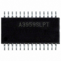
A3959SLP-T Allegro Microsystems Inc, A3959SLP-T Datasheet

A3959SLP-T
Specifications of A3959SLP-T
Available stocks
Related parts for A3959SLP-T
A3959SLP-T Summary of contents
Page 1
Features and Benefits ▪ ± Output Rating ▪ Low r Outputs (270 mΩ, Typical) DS(on) ▪ Mixed, Fast, and Slow Current-Decay Modes ▪ Synchronous Rectification for Low Power Dissipation ▪ Internal UVLO and Thermal-Shutdown Circuitry ▪ Crossover-Current ...
Page 2
... Part Number A3959SB-T 24-pin DIP with exposed tabs A3959SLB-T 24-pin SOIC with internally fused pins A3959SLBTR-T 24-pin SOIC with internally fused pins A3959SLP-T 28-pin TSSOP with exposed thermal pad A3959SLPTR-T 28-pin TSSOP with exposed thermal pad Absolute Maximum Ratings Characteristic Symbol ...
Page 3
A3959 Thermal Characteristics Characteristic Package Power Dissipation Package Thermal Resistance, Junction to Ambient Package Thermal Resistance, Junction to Tab Package Thermal Resistance, Junction to Pad *Additional thermal information available on Allegro website. DMOS Full-Bridge PWM Motor Driver Symbol Test Conditions ...
Page 4
A3959 ELECTRICAL CHARACTERISTICS < 50 kHz (unless noted otherwise) PWM Characteristics Output Drivers Load Supply Voltage Range Output Leakage Current Output On Resistance Crossover Delay Body Diode Forward Voltage Load Supply Current Control Logic Logic Supply Voltage ...
Page 5
A3959 ELECTRICAL CHARACTERISTICS (continued < 50 kHz (unless noted otherwise) PWM Characteristics Reference Divider Ratio Gm Error (Note 3) Propagation Delay Times Thermal Shutdown Temp. Thermal Shutdown Hysteresis UVLO Enable Threshold UVLO Hysteresis NOTES: 1. Typical Data ...
Page 6
A3959 . This internally generated voltage is used to operate V REG the sink-side DMOS outputs. The V be decoupled with a 0.22 μF capacitor to ground. V internally monitored and in the case of a fault condition, the outputs ...
Page 7
A3959 Internal Current-Control Mode. Inputs PFD1 and PFD2 determine the current-decay method after an overcurrent event is detected at the SENSE input. In slow- decay mode, both sink drivers are turned on for the fi xed off-time period. Mixed-decay mode ...
Page 8
A3959 Current Sensing. To minimize inaccuracies in sensing the I current level, which may be caused by TRIP ground trace IR drops, the sense resistor should have an independent ground return to the ground terminal of the device. For low-value ...
Page 9
A3959 (DIP) Package CHARGE PUMP REG ı θ SLEEP PHASE 3 22 ROSC 4 21 OUT LOAD V GROUND SUPPLY GROUND 6 19 GROUND 18 GROUND ...
Page 10
A3959 1.27 MIN +0.25 1.52 –0.38 15.40±0. 24X 0.10 C 0.41 ±0.10 For reference only Pins 6 and 7, and 18 and 19 internally fused Dimensions in millimeters (Reference JEDEC MS-013 AD) Dimensions ...
Page 11
A3959 9.70 ±0. 5.00 28X 0.10 C +0.05 0.25 0.65 –0.06 Copyright ©2001-2008, Allegro MicroSystems, Inc. The products described here are manufactured under one or more U.S. patents or U.S. patents pending. Allegro MicroSystems, Inc. ...


