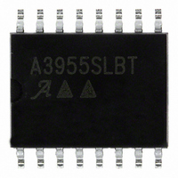
A3955SLB-T Allegro Microsystems Inc, A3955SLB-T Datasheet - Page 10

A3955SLB-T
Manufacturer Part Number
A3955SLB-T
Description
IC MOTOR DRIVER PWM FULL 16-SOIC
Manufacturer
Allegro Microsystems Inc
Datasheet
1.A3955SB-T.pdf
(14 pages)
Specifications of A3955SLB-T
Applications
Stepper Motor Driver
Number Of Outputs
1
Current - Output
±1.5A
Voltage - Load
4.5 V ~ 50 V
Voltage - Supply
4.5 V ~ 5.5 V
Operating Temperature
-20°C ~ 85°C
Mounting Type
Surface Mount
Package / Case
16-SOIC (0.300", 7.5mm Width)
Motor Type
Full Bridge
No. Of Outputs
2
Output Current
1.5A
Output Voltage
50V
Supply Voltage Range
4.5V To 5.5V
Driver Case Style
SOIC
No. Of Pins
16
Operating Temperature Range
-20°C To
Rohs Compliant
Yes
Lead Free Status / RoHS Status
Lead free / RoHS Compliant
Other names
620-1068
A3955
Mixed Current-Decay Mode
and 3.1 V, the device will be in a mixed current-decay mode.
Mixed-decay mode allows the user to achieve good current
regulation with a minimum amount of ripple current and
motor/driver losses by selecting the minimum percentage of fast
decay required for their application (see also the Stepper Motor
Applications section).
As in fast current-decay mode, mixed-decay starts with the sink
and source drivers disabled after the load current reaches I
When the voltage at the RC terminal decays to a value below
V
current-decay mode for the remainder of the fi xed off-time
(fi gure 2). The percentage of fast decay (PFD) is user determined
by V
where:
Fixed Off-Time.
uses a one shot to control the time the driver(s) remain(s) off.
The one-shot off-time, t
an external resistor (R
RC timing terminal to ground. The off-time, over a range of
values of C
approximated by:
When the load current is increasing, but has not yet reached the
sense-current comparator threshold (I
RC terminal is approximately 0.6V
the PWM latch is reset by the current-sense comparator and
the voltage on the RC terminal will decay until it reaches
approximately 0.22V
re-enabling the driver(s) and allowing load current to increase
again. The PWM cycle repeats, maintaining the peak load
current at the desired value.
PFD
PFD
, the sink drivers are re-enabled, placing the device in slow
or two external resistors.
T
= 470 pF to 1500 pF and R
PFD = 100 ln (0.6[R
The internal PWM current-control circuitry
CC
T
) and capacitor (C
. The PWM latch is then set, thereby
OFF
R 1
R 2
V
t
, is determined by the selection of
OFF
CC
≈ R
T
D
CC
. If V
C
T
Full-Bridge PWM Microstepping Motor Driver
TRIP
. When I
1
.
+R
EP 062
PFD
T
PFD
T
), the voltage on the
= 12 kΩ to 100 kΩ, is
2
) connected from the
]/R
is between 1.1 V
2
TRIP
)
is reached,
TRIP
.
With increasing values of t
low-level load-current regulation will improve, EMI will be
reduced, the PWM frequency will decrease, and ripple current
will increase. A value of t
of these parameters. For applications where audible noise is a
concern, typical values of t
15 to 35 μs.
RC Blanking.
the PWM control circuit, the C
blanking time. This function blanks the output of the current-
sense comparator when the outputs are switched by the internal
current-control circuitry (or by the PHASE input, or when the
device is enabled with the DAC data inputs). The comparator
output is blanked to prevent false over-current detections due to
reverse recovery currents of the clamp diodes, and/or switching
transients related to distributed capacitance in the load.
During internal PWM operation, at the end of the t
comparator’s output is blanked and C
from approximately 0.22V
approximately 1 mA. The comparator output remains blanked
until the voltage on C
blanking time, t
When a transition of the PHASE input occurs, C
to near ground during the crossover delay time (the crossover
delay time is present to prevent simultaneous conduction of
the source and sink drivers). After the crossover delay, C
charged by an internal current source of approximately 1 mA.
The comparator output remains blanked until the voltage on C
reaches approximately 0.6V
Similarly, when the device is disabled, via the DAC data inputs,
C
C
mA. The comparator output remains blanked until the voltage on
C
can be calculated as:
The minimum recommended value for C
This value ensures that the blanking time is suffi cient to avoid
false trips of the comparator under normal operating conditions.
For optimal regulation of the load current, this value for C
recommended and the value of R
T
T
T
is discharged to near ground. When the device is re-enabled,
is charged by an internal current source of approximately 1
reaches approximately 0.6V
t
BLANK
t
BLANK
BLANK
In addition to determining the fi xed off-time of
= R
T
T
, can be calculated as:
= R
C
reaches approximately 0.6V
T
OFF
T
ln ([R
115 Northeast Cutoff
1.508.853.5000; www.allegromicro.com
CC
Allegro MicroSystems, Inc.
Worcester, Massachusetts 01615-0036 U.S.A.
OFF,
OFF
C
CC
T
can be chosen for optimization
by an internal current source of
ln (R
.
are chosen to be in the range of
switching losses will decrease,
T
CC
T
component sets the comparator
T
- 1.1 kΩ]/R
. The blanking time, t
can be sized to determine t
T
/[R
T
begins to be charged
T
T
– 3 kΩ]).
is 470 pF ± 5 %.
T
- 3 kΩ).
T
is discharged
OFF
CC
. The
time, the
BLANK
T
T
is
is
,
OFF
T
9
.


