LMD18201T/NOPB National Semiconductor, LMD18201T/NOPB Datasheet - Page 5
LMD18201T/NOPB
Manufacturer Part Number
LMD18201T/NOPB
Description
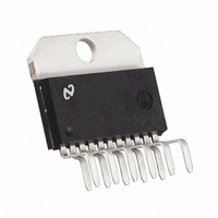
IC H BRIDGE 3A 55V TO220-11
Manufacturer
National Semiconductor
Specifications of LMD18201T/NOPB
Applications
DC Motor Driver, Stepper Motor Driver, H Bridge
Number Of Outputs
1
Current - Output
3A
Voltage - Supply
12 V ~ 55 V
Operating Temperature
-40°C ~ 125°C
Mounting Type
Through Hole
Package / Case
TO-220-11 (Bent and Staggered Leads)
Lead Free Status / RoHS Status
Lead free / RoHS Compliant
Voltage - Load
-
Lead Free Status / Rohs Status
RoHS Compliant part
Electrostatic Device
Other names
*LMD18201T
*LMD18201T/NOPB
LMD18201T
*LMD18201T/NOPB
LMD18201T


Test Circuit
Switching Time Definitions
Pinout Description
gram)
Pin 1, BOOTSTRAP 1 Input: Bootstrap capacitor pin for half
H-Bridge number 1. The recommended capacitor (10 nF) is
connected between pins 1 and 2.
Pin 2, OUTPUT 1: Half H-Bridge number 1 output.
Pin 3, DIRECTION Input: See Table 1. This input controls
the direction of current flow between OUTPUT 1 and OUT-
PUT 2 (pins 2 and 10) and, therefore, the direction of rotation
of a motor load.
Pin 4, BRAKE Input: See Table 1. This input is used to
brake a motor by effectively shorting its terminals. When
braking is desired, this input is taken to a logic high level and
it is also necessary to apply logic high to PWM input, pin 5.
The drivers that short the motor are determined by the logic
level at the DIRECTION input (Pin 3): with Pin 3 logic high,
both current sourcing output transistors are ON; with Pin 3
logic low, both current sinking output transistors are ON. All
output transistors can be turned OFF by applying a logic high
to Pin 4 and a logic low to PWM input Pin 5; in this case only
a small bias current (approximately −1.5 mA) exists at each
output pin.
(See Connection Dia-
01079309
01079308
5
Pin 5, PWM Input: See Table 1. How this input (and DIREC-
TION input, Pin 3) is used is determined by the format of the
PWM Signal.
Pin 6, V
Pin 7, POWER GROUND/SENSE Connection: This pin is
the ground return for the power DMOS transistors of the
H-Bridge. The current through the H-Bridge can be sensed
by adding a small, 0.1Ω, sense resistor from this pin to the
power supply ground.
Pin 8, SIGNAL GROUND: This is the ground return for the
internal logic circuitry used to control the PWM switching of
the H-Bridge.
Pin 9, THERMAL FLAG Output: This pin provides the
thermal warning flag output signal. Pin 9 becomes active-low
at 145˚C (junction temperature). However the chip will not
shut itself down until 170˚C is reached at the junction.
Pin 10, OUTPUT 2: Half H-Bridge number 2 output.
Pin 11, BOOTSTRAP 2 Input: Bootstrap capacitor pin for
half H-Bridge number 2. The recommended capacitor
(10 nF) is connected between pins 10 and 11.
Application Information
TYPES OF PWM SIGNALS
The LMD18201 readily interfaces with different forms of
PWM signals. Use of the part with two of the more popular
forms of PWM is described in the following paragraphs.
Simple, locked anti-phase PWM consists of a single, vari-
able duty-cycle signal in which is encoded both direction and
amplitude information (see Figure 2). A 50% duty-cycle
PWM signal represents zero drive, since the net value of
voltage (integrated over one period) delivered to the load is
zero. For the LMD18201, the PWM signal drives the direc-
tion input (pin 3) and the PWM input (pin 5) is tied to logic
high.
PWM
H
H
H
H
L
L
FIGURE 2. Locked Anti-Phase PWM Control
S
Power Supply
Dir
H
X
H
X
L
L
TABLE 1. Logic Truth Table
Brake
H
H
H
L
L
L
Source 1, Sink 2
Sink 1, Source 2
Source 1, Source 2
Source 1, Source 2
Sink 1, Sink 2
NONE
Active Output Drivers
www.national.com
01079304
Related parts for LMD18201T/NOPB
Image
Part Number
Description
Manufacturer
Datasheet
Request
R

Part Number:
Description:
IC, MOTOR CTRL, HALF BRIDGE 3A TO-220-11
Manufacturer:
National Semiconductor
Datasheet:

Part Number:
Description:
National Semiconductor [8-Bit D/A Converter]
Manufacturer:
National Semiconductor
Datasheet:
Part Number:
Description:
National Semiconductor [Media Coprocessor]
Manufacturer:
National Semiconductor
Datasheet:
Part Number:
Description:
Digitally Controlled Tone and Volume Circuit with Stereo Audio Power Amplifier, Microphone Preamp Stage and National 3D Sound
Manufacturer:
National Semiconductor
Datasheet:
Part Number:
Description:
Digitally Controlled Tone and Volume Circuit with Stereo Audio Power Amplifier, Microphone Preamp Stage and National 3D Sound
Manufacturer:
National Semiconductor
Datasheet:
Part Number:
Description:
AC97 Rev 2 Codec with Sample Rate Conversion and National 3D Sound
Manufacturer:
National Semiconductor
Part Number:
Description:
Manufacturer:
National Semiconductor
Datasheet:
Part Number:
Description:
Manufacturer:
National Semiconductor
Datasheet:
Part Number:
Description:
General Purpose, Low Voltage, Low Power, Rail-to-Rail Output Operational Amplifiers
Manufacturer:
National Semiconductor
Datasheet:
Part Number:
Description:
8-bit 20 MSPS flash A/D converter.
Manufacturer:
National Semiconductor
Datasheet:
Part Number:
Description:
Low Noise Quad Operational Amplifier
Manufacturer:
National Semiconductor
Datasheet:
Part Number:
Description:
Quad Differential Line Receivers
Manufacturer:
National Semiconductor
Datasheet:
Part Number:
Description:
Quad High Speed Trapezoidal? Bus Transceiver
Manufacturer:
National Semiconductor
Datasheet:
Part Number:
Description:
Dual Line Receiver
Manufacturer:
National Semiconductor
Datasheet: