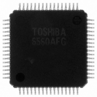
TB6560AFG(O) Toshiba, TB6560AFG(O) Datasheet - Page 28

TB6560AFG(O)
Manufacturer Part Number
TB6560AFG(O)
Description
IC STEPPER MOTOR DRVR 2PH 64HQFP
Manufacturer
Toshiba
Type
Stepper Motor Driverr
Specifications of TB6560AFG(O)
Applications
Stepper Motor Driver, 2 Phase
Number Of Outputs
1
Current - Output
1.5A
Voltage - Load
4.5 V ~ 34 V
Voltage - Supply
4.5 V ~ 5.5 V
Operating Temperature
-30°C ~ 85°C
Mounting Type
Surface Mount
Package / Case
64-QFP Exposed Pad, 64-eQFP, 64-HQFP
Product
Stepper Motor Controllers / Drivers
Operating Supply Voltage
5 V
Mounting Style
SMD/SMT
Motor Type
Stepper
No. Of Outputs
2
Output Current
2.5A
Output Voltage
40V
Supply Voltage Range
4.5V To 5.5V
Driver Case Style
QFP
No. Of Pins
64
Operating Temperature Range
-30°C To +85°C
Rohs Compliant
Yes
Lead Free Status / RoHS Status
Lead free / RoHS Compliant
Other names
TB6560AFGO
TB6560FG
TB6560FG
TB6560FGO
TB6560FG
TB6560FG
TB6560FGO
1. Power-on Sequence with Control Input Signals
2. Power Dissipation
3. Treatment of Heat-Radiating Fin
4. Thermal Shutdown (TSD)
Turn on V
Hold the control input pins Low while turning on V
(All the control input pins are internally pulled down.)
After V
set High. If this sequence is not properly followed, the IC may not operate correctly, or the IC and the
peripheral parts may be damaged.
When RESET is released High, the CLK signal is applied and excitation is started. Only after ENABLE
is also set High, outputs are enabled. When only RESET is set High, outputs are disabled and only the
internal counter advances. Likewise, when only ENABLE is set High, the excitation will not be performed
even if the CLK signal is applied and the outputs will remain in the initial state.
An example of a control input sequence is shown below.
A power-off sequence should be the reverse of this sequence.
<Recommended Control Input Sequence>
The power dissipation of the IC can be calculated by the following equation:
P = V
The higher the ambient temperature, the smaller the power dissipation.
Examine the PD-Ta characteristic curve to determine if there is a sufficient margin in the thermal design.
The heat-radiating fin pins of the TB6560AHQ/AFG (backside) are electrically connected to the backside of
the die. Thus, if a current flows to the fin, the IC may malfunction. If there is any possibility of a voltage
being generated between grounds and the fin, the fin pins should either be connected to ground or
insulated.
When the die temperature reaches 170°C (typ.), the thermal shutdown circuit is tripped, switching the
outputs to off. There is a variation of about ±20°C in the temperature at which the thermal shutdown
circuit is tripped.
Internal current setting
DD
Output current setting
DD
× I
DD
and V
DD
. Then, when the V
+ I
ENABLE
MA/B
OUT
RESET
OUT
CLK
× I
completely stabilizes at the rated voltages, the RESET and ENABLE pins can be
OUT
H
H
H
L
L
L
× Ron × 2 phases
Internal current setting: Disabled;
DD
voltage has stabilized, turn on V
Output OFF
Z
Z
28
DD
and V
MA/B
.
MA/B
Internal current setting: Enabled
Output
.
TB6560AHQ/AFG
2009-07-10


