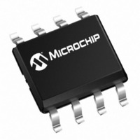
TC646EUA713 Microchip Technology, TC646EUA713 Datasheet - Page 3

TC646EUA713
Manufacturer Part Number
TC646EUA713
Description
IC PWM FAN SPEED CONTRLR 8-MSOP
Manufacturer
Microchip Technology
Type
Controller - PWM Fanr
Datasheet
1.TC646VOA.pdf
(28 pages)
Specifications of TC646EUA713
Applications
Fan Controller, Brushless (BLDC)
Number Of Outputs
1
Voltage - Supply
3 V ~ 5.5 V
Operating Temperature
-40°C ~ 85°C
Mounting Type
Surface Mount
Package / Case
8-MSOP, Micro8™, 8-uMAX, 8-uSOP,
Product
Fan / Motor Controllers / Drivers
Operating Supply Voltage
3 V to 5.5 V
Supply Current
1 mA
Mounting Style
SMD/SMT
Lead Free Status / RoHS Status
Lead free / RoHS Compliant
Current - Output
-
Voltage - Load
-
Lead Free Status / Rohs Status
Lead free / RoHS Compliant
Available stocks
Company
Part Number
Manufacturer
Quantity
Price
Company:
Part Number:
TC646EUA713
Manufacturer:
MICROCHIP
Quantity:
12 000
1.0
Absolute Maximum Ratings*
Supply Voltage ......................................................... 6V
Input Voltage, Any Pin..... (GND – 0.3V) to (V
Package Thermal Resistance:
Specified Temperature Range ........... -40°C to +125°C
Storage Temperature Range.............. -65°C to +150°C
DC ELECTRICAL SPECIFICATIONS
Electrical Characteristics: Unless otherwise specified, T
V
I
I
I
V
t
t
t
I
I
SENSE Input
V
FAULT Output
V
t
t
t
Note 1:
DD
DD(SHDN)
IN
R
F
SHDN
OL
OH
MP
STARTUP
DIAG
DD
OUT
TH(SENSE)
OL
2002 Microchip Technology Inc.
Symbol
PDIP (R
SOIC (R
MSOP (R
Output
ELECTRICAL
CHARACTERISTICS
Ensured by design, not tested.
JA
JA
Supply Voltage
Supply Current, Operating
Supply Current, Shutdown/
Auto-shutdown Mode
V
V
V
Pulse Width(On V
Fault Mode
Sink Current at V
Source Current at V
Output
SENSE Input Threshold
Voltage with Respect to GND
Output Low Voltage
Missing Pulse Detector Timer
Start-up Timer
Diagnostic Timer
JA
)............................................. 125°C/W
) ............................................ 155°C/W
IN
OUT
OUT
) .......................................... 200°C/W
, V
AS
Rise Time
Fall Time
Input Leakage
Parameter
OUT
IN
) to Clear
OUT
Output
DD
+0.3V)
Min
-1.0
3.0
1.0
5.0
—
—
—
—
30
50
—
—
—
—
MIN
T
A
T
MAX
32/F
32/F
Typ
*Stresses above those listed under "Absolute Maximum Rat-
ings" may cause permanent damage to the device. These are
stress ratings only and functional operation of the device at
these or any other conditions above those indicated in the
operation sections of the specifications is not implied. Expo-
sure to absolute maximum rating conditions for extended peri-
ods may affect device reliability.
3/F
0.5
25
70
—
—
—
—
—
—
—
—
, V
DD
= 3.0V to 5.5V
Max
+1.0
0.3
5.5
1.0
90
—
—
—
50
50
—
—
—
—
Units
µsec I
µsec I
µsec V
Sec
Sec
Sec
mA
mV
µA
mA
mA
µA
V
V
Pins 6, 7 Open,
C
Pins 6, 7 Open;
Note 1
C
Note 1
Specifications,
Note 1
V
V
Note 1
I
C
C
C
OH
OL
OL
SHDN
OL
OH
F
F
F
F
F
= 1 µF, V
=1 µF, V
= 1.0 µF
= 1.0 µF
= 1.0 µF
= 1 mA, Note 1
= 2.5 mA
= 5 mA, Note 1
= 10% of V
= 80% of V
Test Conditions
, V
HYST
DS21446C-page 3
TC646
IN
IN
= 0.35V
= V
DD
DD
C(MAX)


