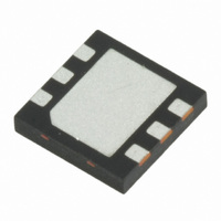
CBC012-D5C-TR1 Cymbet Corporation, CBC012-D5C-TR1 Datasheet - Page 3

CBC012-D5C-TR1
Manufacturer Part Number
CBC012-D5C-TR1
Description
IC BATT SOLID ST ENERCHIP 6DFN
Manufacturer
Cymbet Corporation
Series
EnerChip™r
Datasheet
1.CBC012-D5C-TR1.pdf
(5 pages)
Specifications of CBC012-D5C-TR1
Voltage - Output
3.8V
Capacity
12µAh
Operating Temperature
-20°C ~ 70°C
Package / Case
6-DFN
Battery Cell Size
5 mm x 5 mm
Output Voltage
3.8 V
Termination Style
SMD/SMT
Lead Free Status / RoHS Status
Lead free / RoHS Compliant
Lead Free Status / RoHS Status
Lead free / RoHS Compliant, Lead free / RoHS Compliant
Other names
859-1011-2
CBC012-D5C-TR1
CBC012-D5C-TR1
Printed Circuit Board (PCB) Layout Guidelines and Recommendations
Electrical resistance of solder flux residue on PCBs can be low enough to partially or fully discharge the backup
energy cell and in some cases can be comparable to the load typically imposed on the cell when delivering
power to an integrated circuit in low power mode. Therefore, solder flux must be thoroughly washed from the
board following soldering.
The PCB layout can make this problem worse if the cell’s positive and negative terminals are routed near each
other and under the package, where it is difficult to wash the flux residue away. An undesirable example is
shown in Figure 1. The negative connection on the EnerChip is routed from the negative pad to a via placed
under the package near the positive pad. In this scenario, solder flux residue can wick from the positive solder
pad, covering both the positive pad and the via. This results in a high resistance current path between the
EnerChip terminals. This current path will make the cell appear to be defective or make the application circuit
appear to be drawing too much current.
To avoid this situation, make sure positive and negative traces are routed outside of the package footprint,
as shown in Figure 2, to ensure that flux residue will not cause a discharge path between the positive and
negative pads.
Similarly, a leakage current path can exist from the package lead solder pads to the exposed die pad on the
underside of the package as well as any solder pad on the PCB that would be connected to that exposed die
pad during the reflow solder process. Therefore, it is strongly recommended that the PCB layout not include a
solder pad in the region where the exposed die pad of the package will land. It is sufficient to place PCB solder
pads only where the package leads will be. That region of the PCB where the exposed die pad will land must
not have any solder pads, traces, or vias.
DS-72-02 Rev A
Package Dimensions - 6-pin DFN (package code D5)
Pin Number(s)
Note: NIC = No Internal Connection
©2009-2010Cymbet Corporation • Tel: +1-763-633-1780 • www.cymbet.com
2,3,4,5
1
6
EnerChip™ CBC012 Solid State Energy Storage
Description
NIC
V+
V-
Notes:
1. All linear dimensions are in millimeters.
2. Drawing is subject to change without notice.
Page 3 of 5


