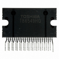
TB6549HQ Toshiba, TB6549HQ Datasheet - Page 7

TB6549HQ
Manufacturer Part Number
TB6549HQ
Description
IC DRIVER FULL BRIDGE 25HZIP
Manufacturer
Toshiba
Type
Full Bridge Motor Driverr
Datasheet
1.TB6549FGOEL.pdf
(22 pages)
Specifications of TB6549HQ
Applications
DC Motor Driver, H Bridge
Number Of Outputs
2
Voltage - Supply
10 V ~ 27 V
Operating Temperature
-20°C ~ 85°C
Mounting Type
Through Hole
Package / Case
25-HZIP
Operating Supply Voltage
10 V to 27 V
Supply Current
10 mA
Mounting Style
Through Hole
Functions
Driver
Vopmax (vm*)
27V (30V)
Io (lpeak)
3.5A (4.5A)
Channel
1-ch
Pwm Drive
direct PWM
Package
HZIP25
Rohs Compatible†
yes‡
Lead Free Status / RoHS Status
Lead free / RoHS Compliant
Current - Output
-
Voltage - Load
-
Lead Free Status / Rohs Status
Lead free / RoHS Compliant
Other names
TB6549HQ(O)
Available stocks
Company
Part Number
Manufacturer
Quantity
Price
Company:
Part Number:
TB6549HQ
Manufacturer:
Toshiba
Quantity:
22
Part Number:
TB6549HQ
Manufacturer:
TOSHIBA/东芝
Quantity:
20 000
Note: Be sure to set the pin PWM to High when the PWM control function is not used.
2. Standby Circuit
OUT1
•
•
•
All circuits are turned off except the standby circuit and the charge pump circuit under the standby
condition.
The input voltage range is shown below. Input at CMOS and TTL level is possible. The input signal has
0.2 V (typ.) hysteresis.
Do not attempt to the control the output by inputting PWM signals to the standby pin. Doing so may
cause the output signal to become unstable, resulting in destruction of the IC. (The charge pump circuit
is turned ON/OFF by the switch of the input signal from the standby pin. If the switching cycle is
shorter than 50 ms, the charge pump circuit will not operate with precise timing. Therefore the
switching cycle of the standby pin should be longer than 50 ms.) When the Standby condition is changed
to Operation Mode, set IN1 and IN2 to Low level (Stop Mode) at first. Then switch IN1 and IN2 to High
level when the charge pump circuit reaches the stable condition, i.e., when VcpA is about V
PWM ON
Output voltage
V
V
M
t1
waveform
INSH
INSL
(OUT1)
OUT1
: GND to 0.8 V
: 2 to V
PWM OFF → ON
t4 = 300 ns (typ.)
V
GND
reg
CC
SB
V
M
V
t1
DD
OUT1
t2
V
GND
t3
PWM ON → OFF
t2 = 300 ns (typ.)
CC
100 kΩ
t4
M
7
t5
OUT1
V
DD
V
GND
CC
PWM ON
t5
M
OUT1
V
GND
CC
V
GND
CC
PWM OFF
TB6549FG/PG/HQ
M
t3
2010-07-13
CC
V
GND
CC
+ 5 V.


