SA12 Cirrus Logic Inc, SA12 Datasheet - Page 4
SA12
Manufacturer Part Number
SA12
Description
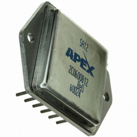
AMP PWM SW 200V 15A 12-DIP CR
Manufacturer
Cirrus Logic Inc
Series
Apex Precision Power™r
Datasheet
1.SA12.pdf
(5 pages)
Specifications of SA12
Mfg Application Notes
SAxx App Note 34
Applications
PWM Motor Driver
Number Of Outputs
1
Current - Output
15A
Voltage - Load
16 V ~ 200 V
Voltage - Supply
14 V ~ 16 V
Operating Temperature
-55°C ~ 125°C
Mounting Type
Through Hole
Package / Case
12-DIP Module
For Use With
598-1461 - EVALUATION FOR SA12
Lead Free Status / RoHS Status
Request inventory verification / Request inventory verification
Other names
598-1364
Available stocks
Company
Part Number
Manufacturer
Quantity
Price

Part Number:
SA12
Manufacturer:
APEX
Quantity:
20 000
Company:
Part Number:
SA12-5S600
Manufacturer:
ARTESYN
Quantity:
228
Part Number:
SA120
Manufacturer:
LRC/乐山
Quantity:
20 000
Company:
Part Number:
SA120A
Manufacturer:
VISHAY
Quantity:
500 000
Part Number:
SA120A
Manufacturer:
VISHAY/威世
Quantity:
20 000
Company:
Part Number:
SA120A-E3/54
Manufacturer:
VISHAY
Quantity:
54 000
Part Number:
SA120CA
Manufacturer:
VISHAY/威世
Quantity:
20 000
Part Number:
SA1220CP
Manufacturer:
NS/国半
Quantity:
20 000


SA12
GENERAL
to Application Note 1 "General Operating Considerations" for
helpful information regarding power supplies, heat sinking
and mounting. Visit www.Cirrus.com for design tools that help
automate pwm filter design; heat sink selection; Apex Precision
Power’s complete Application Notes library; Technical Seminar
Workbook; and Evaluation Kits.
CLOCK CIRCUIT AND RAMP GENERATOR
proximately 400kHz. The CLK OUT pin will normally be tied
to the CLK IN pin. The clock is divided by two and applied to
an RC network which produces a ramp signal at the –PWM/
RAMP pin. An external clock signal can be applied to the CLK
IN pin for synchronization purposes. If a clock frequency lower
than 400kHz is chosen an external capacitor must be tied to
the –PWM/RAMP pin. This capacitor, which parallels an internal
capacitor, must be selected so that the ramp oscillates 4 volts
p-p with the lower peak 3 volts above ground.
PWM INPUTS
comparator. When +PWM > -PWM then A OUT > B OUT. A
motion control processor which generates the pwm signal can
drive these pins with signals referenced to GND.
PROTECTION CIRCUITS
Should either of the outputs be shorted to ground the high
side current limit will latch off the output transistors. The tem-
perature of the output transistors is also monitored. Should a
fault condition raise the temperature of the output transistors
to 165°C the thermal protection circuit will latch off the output
transistors. The latched condition can be cleared by either
recycling the V
with a 10V pulse. See Figures A and B. The outputs will remain
off as long as the shutdown pulse is high (10V).
protect the FET switches in the case of short circuits directly
at the pins of the amplifier. However, a small inductance be-
tween the amplifier and the short circuit will limit current rise
time and the protection circuits will be effective. A pair of 12
inch wires is adequate inductance.
CURRENT LIMIT
sensing pins, I SENSE A and
I SENSE B. The two pins can
be shorted in the voltage
mode connection but both
must be used in the current
mode connection (see figures
A and B). It is recommended
that R
inductive. Load current flows
in the I SENSE pins. To avoid errors due to lead lengths connect
the I LIMIT/SHDN pin directly to the R
the filter network and shutdown divider resistor) and connect
4
Please read Application Note 30 on "PWM Basics". Refer
The clock frequency is internally set to a frequency of ap-
The full bridge driver may be accessed via the pwm input
When supply voltage is over 100V, these circuits may not
There are two load current
A fixed internal current limit senses the high side current.
LIMIT
resistors be non-
cc
power or by toggling the I LIMIT/SHDN input
I LIMIT/SHDN R
FIGURE A. CURRENT LIMIT WITH
SHUTDOWN VOLTAGE MODE.
I SENSE A
I SENSE B
LIMIT
C FILTER
FILTER
resistors (through
R LIMIT
IN4148
5K
SHUTDOWN
SIGNAL
0/10V
P r o d u c t I n n o v a t i o n F r o m
switching circuits it may be difficult to determine the true noise
amplitude without careful attention to grounding of the oscil-
loscope probe. Use the shortest possible ground lead for the
probe and connect exactly at the GND terminal of the amplifier.
Suggested starting values are C
culated by:
maximum desired current. In current mode the required value
of each R
divided down by 2 (see Figure B). If R
divide down the sense voltage. The shutdown divider network
will also have an effect on the filtering circuit.
BYPASSING
proper operation. Failure to do so can cause erratic and low
efficiency operation as well as excessive ringing at the out-
puts. The Vs supply should be bypassed with at least a 1µF
ceramic capacitor in parallel with another low ESR capacitor
of at least 10µF per amp of output current. Capacitor types
rated for switching applications are the only types that should
be considered. The bypass capacitors must be physically
connected directly to the power supply pins. Even one inch of
lead length will cause excessive ringing at the outputs. This
is due to the very fast switching times and the inductance of
the lead connection. The bypassing requirements of the Vcc
supply are less stringent, but still necessary. A .1µF to .47µF
ceramic capacitor connected directly to the Vcc pin will suffice.
MODULATION RANGE
bootstrap circuit. For the output circuit to switch high, the low
side circuit must have previously been switched on in order to
charge the bootstrap capacitor. Therefore, if the input signal
to the SA12 demands a 100% duty cycle upon start-up the
output will not follow and will be in a tri-state (open) condition.
The ramp signal must cross the input signal at some point to
correctly determine the output state. After the ramp crosses the
input signal one time the output state will be correct thereafter.
In addition, if during normal operation the input signal drives
the SA12 beyond its linear modulation range (approximately
95%) the output will jump to 100% modulation.
I LIMIT/SHDN R
FIGURE B. CURRENT LIMIT WITH
SHUTDOWN CURRENT MODE.
I SENSE A
I SENSE B
The required value of R
where R
Adequate bypassing of the power supplies is required for
The high side of the all N channel H-bridge is driven by a
R LIMIT
LIMIT
LIMIT
C FILTER
FILTER
R
is 2 times this value since the sense voltage is
LIMIT
is the required resistor value, and I
R LIMIT
5K
5K
= .1 V / I
IN4148
LIMIT
the R
GND pin.
variably be found at the I SENSE
pins. The noise spikes could trip
the current limit threshold which
is only 100 mV. R
should be adjusted so as to reduce
LIMIT
SHUTDOWN
Switching noise spikes will in-
SIGNAL
in voltage mode may be cal-
FILTER
0/10V
LIMIT
SHDN
resistors directly to the
= .01uF, R
the switching noise well
below 100 mV to prevent
false current limiting.
The sum of the DC level
plus the noise peak will
determine the current
limiting value. As in most
is used it will further
FILTER
FILTER
and C
LIMIT
= 5k .
SA12U
is the
FILTER
Related parts for SA12
Image
Part Number
Description
Manufacturer
Datasheet
Request
R

Part Number:
Description:
Development Kit
Manufacturer:
Cirrus Logic Inc
Datasheet:
Part Number:
Description:
Development Kit
Manufacturer:
Cirrus Logic Inc
Datasheet:


Part Number:
Description:
High-efficiency PFC + Fluorescent Lamp Driver Reference Design
Manufacturer:
Cirrus Logic Inc
Datasheet:
Part Number:
Description:
Development Kit
Manufacturer:
Cirrus Logic Inc
Datasheet:
Part Number:
Description:
Development Kit
Manufacturer:
Cirrus Logic Inc
Datasheet:

Part Number:
Description:
Development Kit
Manufacturer:
Cirrus Logic Inc
Datasheet:
Part Number:
Description:
Development Kit
Manufacturer:
Cirrus Logic Inc
Datasheet:
Part Number:
Description:
Development Kit
Manufacturer:
Cirrus Logic Inc
Datasheet:
Part Number:
Description:
Development Kit
Manufacturer:
Cirrus Logic Inc
Datasheet:

Part Number:
Description:
EVALUATION BOARD FOR CS8427
Manufacturer:
Cirrus Logic Inc
Datasheet:

Part Number:
Description:
BOARD EVAL FOR CS8416 RCVR
Manufacturer:
Cirrus Logic Inc
Datasheet:

Part Number:
Description:
EVALUATION BOARD FOR CS8420
Manufacturer:
Cirrus Logic Inc
Datasheet:

Part Number:
Description:
KIT DEVELOPMENT EP9315 ARM9
Manufacturer:
Cirrus Logic Inc
Datasheet:

Part Number:
Description:
KIT DEVELOPMENT EP9302 ARM9
Manufacturer:
Cirrus Logic Inc
Datasheet: