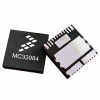
MC33984BPNA Freescale Semiconductor, MC33984BPNA Datasheet - Page 27

MC33984BPNA
Manufacturer Part Number
MC33984BPNA
Description
IC SWITCH HI SIDE DUAL 16-PQFN
Manufacturer
Freescale Semiconductor
Type
High Sider
Datasheet
1.MC33984BPNAR2.pdf
(38 pages)
Specifications of MC33984BPNA
Input Type
SPI
Number Of Outputs
2
On-state Resistance
4 mOhm
Voltage - Supply
6 V ~ 27 V
Operating Temperature
-40°C ~ 125°C
Mounting Type
Surface Mount
Package / Case
16-PQFN, 16-PowerQFN
Lead Free Status / RoHS Status
Lead free / RoHS Compliant
Current - Output / Channel
-
Current - Peak Output
-
Available stocks
Company
Part Number
Manufacturer
Quantity
Price
Part Number:
MC33984BPNA
Manufacturer:
FREESCALE
Quantity:
20 000
SERIAL OUTPUT COMMUNICATION
(DEVICE STATUS RETURN DATA)
loaded. Meanwhile, the data is clocked out MSB- (OD7-) first
as the new message data is clocked into the SI pin. The first
eight bits of data clocking out of the SO, and following a
transition, are dependant upon the previously written SPI
word.
be representative of the initial message bits clocked into the
SI pin since the
feature is useful for daisy chaining devices as well as
message verification.
transition of Logic [0] to Logic [1]. If there is a valid message
length, the data is latched into the appropriate registers. A
valid message length is a multiple of eight bits. At this time,
the SO pin is tri-stated and the fault status register is now
able to accept new fault status information.
the STATR-selected register data at the time that the
pulled to a Logic [0] during SPI communication and / or for the
period of time since the last valid SPI communication, with
the following exceptions:
Table 16. Serial Output Bit Map Description
Analog Integrated Circuit Device Data
Freescale Semiconductor
SOA3 SOA2 SOA1 SOA0
s = Selection of output: Logic [0] = HS0, Logic [1] = HS1.
x = Don’t care.
When the
Any bits clocked out of the SO pin after the first eight will
A valid message length is determined following a
The output status register correctly reflects the status of
• The previous SPI communication was determined to be
• Battery transients below 6.0 V resulting in an under-
• The
s
x
s
s
s
0
1
0
1
x
Previous STATR
invalid. In this case, the status will be reported as
though the invalid SPI communication never occurred.
voltage shutdown of the outputs may result in incorrect
data loaded into the status register. The SO data
transmitted to the MCU during the first SPI
communication following an under-voltage V
condition should be ignored.
the WAKE pin is at Logic [0] may result in incorrect data
loaded into the status register. The SO data transmitted
D7, D2, D1, D0
0
0
0
0
1
1
1
1
1
1
RST
CS
pin transition from a Logic [0] to Logic [1] while
0
0
1
1
0
0
0
1
1
1
CS
pin is pulled low, the output status register is
pin first transitioned to a Logic [0]. This
0
1
0
1
0
1
1
0
0
1
OD7
0
1
0
1
–
s
x
s
s
s
OTFs
OD6
0
0
0
1
1
1
1
1
–
PWR
CS
CS
OCHFs
OD5
CS
0
1
1
0
0
0
1
1
–
is
Serial Output Returned Data
SERIAL OUTPUT BIT ASSIGNMENT
serial input message, as explained in the following
paragraphs.
addressed during the prior communication. The value of the
previous D7 will determine which output the status
information applies to for the Fault (FLTR), SOCHLR,
CDTOLR, and DICR registers. SO data will represent
information ranging from fault status to register contents,
user selected by writing to the STATR bits D2:D0. Note that
the SO data will continue to reflect the information for each
output (depending on the previous D7 state) that was
selected during the most recent STATR write until changed
with an updated STATR write.
Previous Address SOA[2:0] = 000
reflect the current state of the Fault register (FLTR)
corresponding to the output previously selected with the bit
OD7
Previous Address SOA[2:0] = 001
programmed bits, respectively. Data in bits OD3:OD2 contain
CSNS0
Previous Address SOA[2:0] = 010
high detection level (refer to
OD2:OD0 contain the programmed over-current low
detection levels (refer to
OCLFs
OD4
1
0
1
0
1
1
0
0
–
The 8 bits of serial output data depend on the previous
Bit OD7 reflects the state of the watchdog bit (D7)
If the previous three MSBs are 000, bits OD6 : OD0 will
Data in bits OD1:OD0 contain CSNS0
The data in bit OD3 contain the programmed over-current
(Table
to the MCU during the first SPI communication following
this condition should be ignored.
EN
See
FAST SR s CSNS high s
CSNS1
FSM_HS0
FSM_HS1
OL_DIS s
and IN0_SPI programmed bits, respectively.
17).
SOCHs
IN1 Pin
Table 16
OLFs
OD3
Table 1
–
EN
summarizes the SO register content.
LOGIC COMMANDS AND REGISTERS
CD_DIS s
Table
IN1_SPI
SOCL2s
IN0 Pin
WDTO
OSD2
FUNCTIONAL DEVICE OPERATION
OD2
UVF
–
–
Table
13).
12), and the data in bits
CSNS0
SOCL1s
OCLT1s
IN DIS s
FSI Pin
UV_dis
OSD1
WD1
OD1
OVF
–
EN
EN
and IN0_SPI
WAKE Pin
SOCL0s
IN0_SPI
OCLT0s
FAULT
OV_dis
OSD0
A/O s
WD0
OD0
–
33984
27


